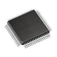
ST92T163R4T1 STMicroelectronics, ST92T163R4T1 Datasheet - Page 35

ST92T163R4T1
Manufacturer Part Number
ST92T163R4T1
Description
Microcontrollers (MCU) OTP EPROM 20K USB/I2
Manufacturer
STMicroelectronics
Datasheet
1.ST92T163R4T1.pdf
(224 pages)
Specifications of ST92T163R4T1
Data Bus Width
8 bit, 16 bit
Program Memory Type
EPROM
Program Memory Size
20 KB
Data Ram Size
2 KB
Interface Type
I2C, SCI, USB
Maximum Clock Frequency
24 MHz
Number Of Programmable I/os
64
Number Of Timers
2
Operating Supply Voltage
4 V to 5.5 V
Maximum Operating Temperature
+ 70 C
Mounting Style
SMD/SMT
Package / Case
TQFP-64
Minimum Operating Temperature
0 C
On-chip Adc
8 bit
Lead Free Status / Rohs Status
No
Available stocks
Company
Part Number
Manufacturer
Quantity
Price
Company:
Part Number:
ST92T163R4T1L
Manufacturer:
ST
Quantity:
444
Part Number:
ST92T163R4T1L
Manufacturer:
ST
Quantity:
20 000
SYSTEM REGISTERS (Cont’d)
2.3.4 Paged Registers
Up to 64 pages, each containing 16 registers, may
be mapped to Group F. These paged registers
hold data and control information relating to the
on-chip peripherals, each peripheral always being
associated with the same pages and registers to
ensure code compatibility between ST9+ devices.
The number of these registers depends on the pe-
ripherals present in the specific ST9 device. In oth-
er words, pages only exist if the relevant peripher-
al is present.
The paged registers are addressed using the nor-
mal register addressing modes, in conjunction with
the Page Pointer register, R234, which is one of
the System registers. This register selects the
page to be mapped to Group F and, once set,
does not need to be changed if two or more regis-
ters on the same page are to be addressed in suc-
cession.
Thus the instructions:
spp #5
ld R242, r4
will load the contents of working register r4 into the
third register of page 5 (R242).
Warning: During an interrupt, the PPR register is
not saved automatically in the stack. If needed, it
should be saved/restored by the user within the in-
terrupt routine.
PAGE POINTER REGISTER (PPR)
R234 - Read/Write
Register Group: E (System)
Reset value: xxxx xx00 (xxh)
Bit 7:2 = PP[5:0]: Page Pointer .
These bits contain the number (in the range 0 to
63) of the page specified in the spp instruction.
Once the page pointer has been set, there is no
need to refresh it unless a different page is re-
quired.
Bit 1:0: Reserved. Forced by hardware to 0.
2.3.5 Mode Register
The Mode Register allows control of the following
operating parameters:
PP5
7
PP4
PP3
PP2
PP1
PP0
0
0
0
– Selection of internal or external System and User
– Management of the clock frequency,
– Enabling of Bus request and Wait signals when
MODE REGISTER (MODER)
R235 - Read/Write
Register Group: E (System)
Reset value: 1110 0000 (E0h)
Bit 7 = SSP: System Stack Pointer .
This bit selects an internal or external System
Stack area.
0: External system stack area, in memory space.
1: Internal system stack area, in the Register File
Bit 6 = USP: User Stack Pointer .
This bit selects an internal or external User Stack
area.
0: External user stack area, in memory space.
1: Internal user stack area, in the Register File (re-
Bit 5 = DIV2: OSCIN Clock Divided by 2 .
This bit controls the divide-by-2 circuit operating
on OSCIN.
0: Clock divided by 1
1: Clock divided by 2
Bit 4:2 = PRS[2:0]: CPUCLK Prescaler .
These bits load the prescaler division factor for the
internal clock (INTCLK). The prescaler factor se-
lects the internal clock frequency, which can be di-
vided by a factor from 1 to 8. Refer to the Reset
and Clock Control chapter for further information.
Bit 1 = BRQEN: Bus Request Enable .
0: External Memory Bus Request disabled
1: External Memory Bus Request enabled on the
Bit 0 = HIMP: High Impedance Enable .
When any of Ports 0, 1, 2 or 6 depending on de-
vice configuration, are programmed as Address
and Data lines to interface external Memory, these
lines and the Memory interface control lines (AS,
SSP
Stack areas,
interfacing to external memory.
(reset state).
set state).
BREQ pin (where available).
7
ST92163 - DEVICE ARCHITECTURE
USP
DIV2
PRS2 PRS1 PRS0 BRQEN HIMP
35/224
0


