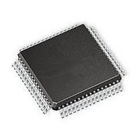
ST92T163R4T1 STMicroelectronics, ST92T163R4T1 Datasheet - Page 198

ST92T163R4T1
Manufacturer Part Number
ST92T163R4T1
Description
Microcontrollers (MCU) OTP EPROM 20K USB/I2
Manufacturer
STMicroelectronics
Datasheet
1.ST92T163R4T1.pdf
(224 pages)
Specifications of ST92T163R4T1
Data Bus Width
8 bit, 16 bit
Program Memory Type
EPROM
Program Memory Size
20 KB
Data Ram Size
2 KB
Interface Type
I2C, SCI, USB
Maximum Clock Frequency
24 MHz
Number Of Programmable I/os
64
Number Of Timers
2
Operating Supply Voltage
4 V to 5.5 V
Maximum Operating Temperature
+ 70 C
Mounting Style
SMD/SMT
Package / Case
TQFP-64
Minimum Operating Temperature
0 C
On-chip Adc
8 bit
Lead Free Status / Rohs Status
No
Available stocks
Company
Part Number
Manufacturer
Quantity
Price
Company:
Part Number:
ST92T163R4T1L
Manufacturer:
ST
Quantity:
444
Part Number:
ST92T163R4T1L
Manufacturer:
ST
Quantity:
20 000
ST92163 - A/D CONVERTER (A/D)
A/D CONVERTER (Cont’d)
The conversion technique used is successive ap-
proximation, with AC coupled analog fully differen-
tial comparators blocks plus a Sample and Hold
logic and a reference generator.
The internal reference (DAC) is based on the use
of a binary-ratioed capacitor array. This technique
allows the specified monotonicity (using the same
ratioed capacitors as sampling capacitor). A Pow-
er Down programmable bit sets the A/D converter
analog section to a zero consumption idle status.
8.6.3.1 Operating Modes
The two main operating modes, single and contin-
uous, can be selected by writing 0 (reset value) or
1 into the CONT bit of the Control Logic Register.
Single Mode
In single mode (CONT=0 in ADCLR) the STR bit is
forced to ’0’ after the end of channel i-th conver-
sion; then the A/D waits for a new start event. This
mode is useful when a set of signals must be sam-
pled at a fixed frequency imposed by a Timer unit
or an external generator (through the alternate
synchronization feature). A simple software rou-
tine monitoring the STR bit can be used to save
the current value before a new conversion ends
(so to create a signal samples table within the in-
ternal memory or the Register File). Furthermore,
if the R242.0 bit (register AD-INT, bit 0) is set, at
the end of conversion a negative edge on the con-
nected external interrupt channel (see Interrupts
Chapter) is generated to allow the reading of the
converted data by means of an interrupt routine.
Continuous Mode
In continuous mode (CONT=1 in ADCLR) a con-
tinuous conversion flow is entered by a start event
on the selected channel until the STR bit is reset
by software.
At the end of each conversion, the Data Register
(ADCDR) content is updated with the last conver-
sion result, while the former value is lost. When the
conversion flow is stopped, an interrupt request is
generated with the same modality previously de-
scribed.
8.6.3.2 Alternate Synchronization
This feature is available in both single/continuous
modes. The negative edge of external EXTRG sig-
nal or the occurrence of an on-chip event generat-
ed by another peripheral can be used to synchro-
nize the conversion start with a trigger pulse.
198/224
These events can be enabled or masked by pro-
gramming the TRG bit in the ADCLR Register.
The effect of alternate synchronization is to set the
STR bit, which is cleared by hardware at the end of
each conversion in single mode. In continuous
mode any trigger pulse following the first one will
be ignored. The synchronization source must pro-
vide a pulse (1.5 internal system clock, 125ns @
12 MHz internal clock) of minimum width, and a
period greater (in single mode) than the conver-
sion time (~6.5us @ 12 MHz internal clock). If a
trigger occurs when the STR bit is still ’1’ (conver-
sions still in progress), it is ignored (see Electrical
Characteristics).
WARNING: If the EXTRG or INTRG signals are al-
ready active when TRG bit is set, the conversion
starts immediately.
8.6.3.3 Power-Up Operations
Before enabling any A/D operation mode, set the
POW bit of the ADCLR Register at least 60 s be-
fore the first conversion starts to enable the bias-
ing circuits inside the analog section of the con-
verter. Clearing the POW bit is useful when the
A/D is not used so reducing the total chip power
consumption. This state is also the reset configu-
ration and it is forced by hardware when the core is
in HALT state (after a HALT instruction execution).
8.6.3.4 Register Mapping
It is possible to have two independent A/D convert-
ers in the same device. In this case they are
named A/D 0 and A/D 1. If the device has one A/D
converter it uses the register addresses of A/D 0.
The register map is the following:
If two A/D converters are present, the registers are
renamed, adding the suffix 0 to the A/D 0 registers
and 1 to the A/D 1 registers.
Register Address
FB-FFh
F3-F7h
F0h
F1h
F2h
F8h
F9h
FAh
A/D 0
A/D 0
A/D 0
A/D 0
A/D 1
A/D 1
A/D 1
A/D 1
ADn
Page 62 (3Eh)
Reserved
Reserved
ADDTR0
ADDTR1
ADCLR0
ADCLR1
ADINT0
ADINT1


