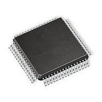
ST92T163R4T1 STMicroelectronics, ST92T163R4T1 Datasheet - Page 193

ST92T163R4T1
Manufacturer Part Number
ST92T163R4T1
Description
Microcontrollers (MCU) OTP EPROM 20K USB/I2
Manufacturer
STMicroelectronics
Datasheet
1.ST92T163R4T1.pdf
(224 pages)
Specifications of ST92T163R4T1
Data Bus Width
8 bit, 16 bit
Program Memory Type
EPROM
Program Memory Size
20 KB
Data Ram Size
2 KB
Interface Type
I2C, SCI, USB
Maximum Clock Frequency
24 MHz
Number Of Programmable I/os
64
Number Of Timers
2
Operating Supply Voltage
4 V to 5.5 V
Maximum Operating Temperature
+ 70 C
Mounting Style
SMD/SMT
Package / Case
TQFP-64
Minimum Operating Temperature
0 C
On-chip Adc
8 bit
Lead Free Status / Rohs Status
No
Available stocks
Company
Part Number
Manufacturer
Quantity
Price
Company:
Part Number:
ST92T163R4T1L
Manufacturer:
ST
Quantity:
444
Part Number:
ST92T163R4T1L
Manufacturer:
ST
Quantity:
20 000
I
INTERRUPT VECTOR REGISTER (I2CIVR)
R249 - Read / Write
Register Page: 20
Reset Value: Undefined
Bit 7:3 = V[7:3] Interrupt Vector Base Address .
User programmable interrupt vector bits. These
are the five more significant bits of the interrupt
vector base address. They must be set before en-
abling the interrupt features.
Bit 2:1 = EV[2:1] Encoded Interrupt Source .
These Read-Only bits are set by hardware accord-
ing to the interrupt source:
– 01: error condition detected
– 10: data received
– 11: peripheral ready to transmit
Bit 0 = Reserved.
Forced by hardware to 0.
RECEIVER DMA SOURCE ADDRESS POINTER
REGISTER (I2CRDAP)
R250 - Read / Write
Register Page: 20
Reset Value: Undefined
Bit 7:1 = RA[7:1] Receiver DMA Address Pointer .
I2CRDAP contains the address of the pointer (in
the Register File) of the Receiver DMA data
source when the DMA is selected between the
peripheral and the Memory Space. Otherwise,
2
RA7 RA6 RA5 RA4 RA3 RA2 RA1
C INTERFACE (Cont’d)
V7
7
7
V6
V5
V4
V3
EV2
EV1
RPS
0
0
0
(DMA between peripheral and Register file), this
register has no meaning.
See Section 8.5.6.1 for more details on the use of
this register.
Bit 0 = RPS Receiver DMA Memory Pointer Selec-
tor .
If memory has been selected for DMA transfer
(DDCRDC.RF/MEM = 0) then:
0: Select ISR register for Receiver DMA transfer
1: Select DMASR register for Receiver DMA trans-
RECEIVER DMA TRANSACTION COUNTER
REGISTER (I2CRDC)
R251 - Read / Write
Register Page: 20
Reset Value: Undefined
Bit 7:1 = RC[7:1] Receiver DMA Counter Pointer.
I2CRDC contains the address of the pointer (in the
Register File) of the DMA receiver transaction
counter when the DMA between Peripheral and
Memory Space is selected. Otherwise (DMA be-
tween Peripheral and Register File), this register
points to a pair of registers that are used as DMA
Address register and DMA Transaction Counter.
See Section 8.5.6.1 and Section 8.5.6.2 for more
details on the use of this register.
Bit 0 = RF/MEM Receiver Register File/ Memory
Selector.
0: DMA towards Memory
1: DMA towards Register file
RC7 RC6 RC5 RC4 RC3 RC2 RC1 RF/MEM
address extension.
fer address extension.
7
ST92163 - I2C BUS INTERFACE
193/224
0


