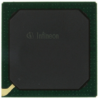
PEB20256E-V21 Infineon Technologies, PEB20256E-V21 Datasheet - Page 97

PEB20256E-V21
Manufacturer Part Number
PEB20256E-V21
Description
IC CONTROLLER INTERFACE 388-BGA
Manufacturer
Infineon Technologies
Datasheet
1.PEB20256E-V21.pdf
(232 pages)
Specifications of PEB20256E-V21
Function
Multichannel Network Interface Controller (MUNICH)
Interface
HDLC, PPP, Serial, TMA
Voltage - Supply
3 V ~ 3.6 V
Current - Supply
200mA
Power (watts)
3W
Operating Temperature
0°C ~ 70°C
Mounting Type
Surface Mount
Package / Case
388-BBGA
Lead Free Status / RoHS Status
Contains lead / RoHS non-compliant
Number Of Circuits
-
Other names
PEB20256E-V21
PEB20256E-V21IN
PEB20256E-V21IN
Available stocks
Company
Part Number
Manufacturer
Quantity
Price
Company:
Part Number:
PEB20256E-V21
Manufacturer:
MAX
Quantity:
63
Company:
Part Number:
PEB20256E-V21
Manufacturer:
Infineon Technologies
Quantity:
10 000
- Current page: 97 of 232
- Download datasheet (3Mb)
transfer, so IRDY is deasserted on clock 7, and FRAME stays asserted. Only when IRDY
is asserted can FRAME be deasserted, which occurs on clock 8.
•
Figure 5-1
5.1.2
The transaction starts when FRAME is activated (clock 1 in Figure 5-2 ). A write
transaction is similar to a read transaction except no turnaround cycle is required
following the address phase. In the example, the first and second data phases complete
with zero wait cycles. The third data phase has three wait cycles inserted by the target.
Both initiator and target insert a wait cycle on clock 5. In the case where the initiator
inserts a wait cycle (clock 5), the data is held on the bus, but the byte enables are
withdrawn. The last data phase is characterized by IRDY being asserted while the
FRAME signal is deasserted. This data phase is completed when TRDY goes active
(clock 8).
Data Sheet
DEVSEL
FRAME
TRDY
IRDY
C/BE
CLK
AD
PCI Write Transaction
PCI Read Transaction
1
Command
Address
Address
phase
2
phase
Data
3
Data 1
4
Bus transaction
97
BE's
phase
Data
5
Data 2
6
Data 3
Interface Description
phase
Data
7
PEB 20256 E
PEF 20256 E
8
04.2001
Related parts for PEB20256E-V21
Image
Part Number
Description
Manufacturer
Datasheet
Request
R

Part Number:
Description:
Manufacturer:
Infineon Technologies AG
Datasheet:

Part Number:
Description:
Manufacturer:
Infineon Technologies AG
Datasheet:

Part Number:
Description:
Manufacturer:
Infineon Technologies AG
Datasheet:

Part Number:
Description:
Manufacturer:
Infineon Technologies AG
Datasheet:

Part Number:
Description:
Manufacturer:
Infineon Technologies AG
Datasheet:

Part Number:
Description:
Manufacturer:
Infineon Technologies AG
Datasheet:

Part Number:
Description:
Manufacturer:
Infineon Technologies AG
Datasheet:

Part Number:
Description:
16-bit microcontroller with 2x2 KByte RAM
Manufacturer:
Infineon Technologies AG
Datasheet:

Part Number:
Description:
NPN silicon RF transistor
Manufacturer:
Infineon Technologies AG
Datasheet:

Part Number:
Description:
NPN silicon RF transistor
Manufacturer:
Infineon Technologies AG
Datasheet:

Part Number:
Description:
NPN silicon RF transistor
Manufacturer:
Infineon Technologies AG
Datasheet:

Part Number:
Description:
NPN silicon RF transistor
Manufacturer:
Infineon Technologies AG
Datasheet:

Part Number:
Description:
Si-MMIC-amplifier in SIEGET 25-technologie
Manufacturer:
Infineon Technologies AG
Datasheet:

Part Number:
Description:
IGBT Power Module
Manufacturer:
Infineon Technologies AG
Datasheet:

Part Number:
Description:
IC for switching-mode power supplies
Manufacturer:
Infineon Technologies AG
Datasheet:


