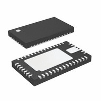
LTC3577EUFF#PBF Linear Technology, LTC3577EUFF#PBF Datasheet - Page 16

LTC3577EUFF#PBF
Manufacturer Part Number
LTC3577EUFF#PBF
Description
IC PWR MANAGEMENT HANDHELD 44QFN
Manufacturer
Linear Technology
Datasheet
1.LTC3577EUFFPBF.pdf
(54 pages)
Specifications of LTC3577EUFF#PBF
Applications
Handheld/Mobile Devices
Voltage - Supply
4.35 V ~ 5.5 V
Operating Temperature
-40°C ~ 85°C
Mounting Type
Surface Mount
Package / Case
44-QFN
Lead Free Status / RoHS Status
Lead free / RoHS Compliant
Current - Supply
-
Available stocks
Company
Part Number
Manufacturer
Quantity
Price
PIN FUNCTIONS
LTC3577/LTC3577-1
I
and I
“USB PowerPath Controller” section. Both pins are pulled
low by a weak current sink.
LED_FS (Pin 3): A resistor between this pin and ground
sets the full-scale output current of the I
WALL (Pin 4): Wall Adapter Present Input. Pulling this
pin above 4.3V will disconnect the power path from V
to V
that a wall adapter has been detected.
SW3 (Pin 5): Power Transmission (Switch) Pin for Step-
Down Switching Regulator 3 (buck3).
V
tor 3. This pin should be connected to V
FB3 (Pin 7): Feedback Input for Step-Down Switching
Regulator 3 (buck3). This pin servos to a fi xed voltage of
0.8V when the control loop is complete.
OVSENSE (Pin 8): Overvoltage Protection Sense Input.
OVSENSE should be connected through a 6.2k resistor
to the input power connector and the drain of an external
N-channel MOS pass transistor. When the voltage on
this pin exceeds a preset level, the OVGATE pin will be
pulled to GND to disable the pass transistor and protect
downstream circuitry.
LED_OV (Pin 9): A resistor between this pin and the boosted
LED backlight voltage sets the overvoltage limit on the
boost output. If the boost voltage exceeds the programmed
limit the LED boost converter will be disabled.
DV
the logic reference level of the LTC3577. A UVLO circuit on
the DV
is <1V. Bypass to GND with a 0.1μF capacitor.
SDA (Pin 11): I
per clock to control the LTC3577. The logic level for SDA
is referenced to DV
SCL (Pin 12): I
referenced to DV
16
LIM0
IN3
CC
OUT
(Pin 6): Power Input for Step-Down Switching Regula-
LIM1
, I
(Pin 10): Supply Voltage for I
CC
LIM1
. The ACPR pin will also be pulled low to indicate
control the input current limit. See Table 1 in the
pin forces all registers to all 0s whenever DV
(Pins 1, 2): Input Current Control Pins. I
2
2
C Data Input. Serial data is shifted one bit
C Clock Input. The logic level for SCL is
CC
.
CC
.
2
C Lines. This pin sets
OUT
LED
.
pin.
LIM0
BUS
CC
OVGATE (Pin 13): Overvoltage Protection Gate Output.
Connect OVGATE to the gate pin of an external N-channel
MOS pass transistor. The source of the transistor should
be connected to V
to the product’s DC input connector. In the absence of an
overvoltage condition, this pin is connected to an internal
charge pump capable of creating suffi cient overdrive to
fully enhance this transistor. If an overvoltage condition
is detected, OVGATE is brought rapidly to GND to prevent
damage. OVGATE works in conjunction with OVSENSE to
provide this protection.
PWR_ON (Pin 14): Logic Input Used to Keep Buck
DC/DCs Enabled After Power-Up. May also be used to
enable the buck DC/DCs directly (sequence = buck1 →
buck2 → buck3). See the “Pushbutton Interface Opera-
tion” section for more information.
ON (Pin 15): Pushbutton Input. A weak internal pull-up
forces ON high when left fl oating. A normally open push-
button is connected from ON to ground to force a low
state on this pin.
PBSTAT (Pin 16): Open-drain output is a de-bounced
and buffered version of ON to be used for processor
interrupts.
WAKE (Pin 17): Open-Drain Output. The WAKE pin indicates
the operating state of the buck DC/DCs. If WAKE is Hi-Z,
the buck DC/DCs are enabled and either up or powering up.
A low on WAKE indicates that the buck DC/DCs are either
powered down or are powering down. See the “Pushbutton
Interface Operation” section for more information.
SW (Pins 18,19,20): Power Transmission (Switch) Pin
for LED Boost Converter. See the “LED Backlight/Boost
Operation” section for circuit hook-up and component
selection. I
default is LED driver off.
PG_DCDC (Pin 21): Open-Drain Output. PG_DCDC goes
high impedance 230ms after all buck DC/DCs are in regula-
tion (within 8% of fi nal value).
2
C is used to control LED driver enable. I
BUS
and the drain should be connected
3577fa
2
C


