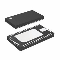
LTC3577EUFF#PBF Linear Technology, LTC3577EUFF#PBF Datasheet - Page 29

LTC3577EUFF#PBF
Manufacturer Part Number
LTC3577EUFF#PBF
Description
IC PWR MANAGEMENT HANDHELD 44QFN
Manufacturer
Linear Technology
Datasheet
1.LTC3577EUFFPBF.pdf
(54 pages)
Specifications of LTC3577EUFF#PBF
Applications
Handheld/Mobile Devices
Voltage - Supply
4.35 V ~ 5.5 V
Operating Temperature
-40°C ~ 85°C
Mounting Type
Surface Mount
Package / Case
44-QFN
Lead Free Status / RoHS Status
Lead free / RoHS Compliant
Current - Supply
-
Available stocks
Company
Part Number
Manufacturer
Quantity
Price
OPERATION
By using a bias resistor, R
the hot and cold trip points can be moved in either direc-
tion. The temperature span will change somewhat due to
the non-linear behavior of the thermistor. The following
equations can be used to easily calculate a new value for
the bias resistor:
where r
sired hot and cold trip points. Note that these equations
are linked. Therefore, only one of the two trip points can
be chosen, the other is determined by the default ratios
designed in the IC.
Consider an example where a 60°C hot trip point is
desired. From the Vishay Curve 1 R-T characteristics,
r
should be set to 46.4k. With this value of R
trip point is about 16°C. Notice that the span is now 44°C
rather than the previous 40°C. This is due to the decrease
in “temperature gain” of the thermistor as absolute tem-
perature increases.
The upper and lower temperature trip points can be inde-
pendently programmed by using an additional bias resistor
as shown in Figure 9. The following formulas can be used
to compute the values of R
For example, to set the trip points to 0°C and 45°C with
a Vishay Curve 1 thermistor choose
the nearest 1% value is 105k.
the nearest 1% value is 12.7k. The fi nal solution is shown
in Figure 9 and results in an upper trip point of 45°C and
a lower trip point of 0°C.
HOT
R1 = 0.536 • 105k – 0.4368 • 100k = 12.6k
R
R
R
R1= 0.536 • R
R
NOM
NOM
NOM
NOM
is 0.2488 at 60°C. Using the above equation, R
HOT
=
=
=
=
r
r
0.538
3.266 – 0.4368
and r
3.17
COLD
r
COLD
HOT
2.714
2.714
COLD
NOM
– r
• R25
• R25
HOT
– r
are the resistance ratios at the de-
HOT
• R25
NOM
NOM
• 100k = 104.2k
• R25
, different in value from R25,
and R1:
NOM
, the cold
NOM
Overvoltage Protection (OVP)
The LTC3577 can protect itself from the inadvertent ap-
plication of excessive voltage to V
two external components: an N-channel FET and a 6.2k
resistor. The maximum safe overvoltage magnitude will
be determined by the choice of the external NMOS and
its associated drain breakdown voltage.
The overvoltage protection module consists of two pins.
The fi rst, OVSENS, is used to measure the externally applied
voltage through an external resistor. The second, OVGATE,
is an output used to drive the gate pin of an external FET.
The voltage at OVSENS will be lower than the OVP input
voltage by (I
escent current. The OVP input will be 200mV to 400mV
higher than OVSENS under normal operating conditions.
When OVSENS is below 6V, an internal charge pump will
drive OVGATE to approximately 1.88 • OVSENS. This will
enhance the N-channel FET and provide a low impedance
connection to V
LTC3577. If OVSENS should rise above 6V (6.35V OVP
input) due to a fault or use of an incorrect wall adapter,
OVGATE will be pulled to GND, disabling the external FET
to protect downstream circuitry. When the voltage drops
below 6V again, the external FET will be re-enabled.
In an overvoltage condition, the OVSENS pin will be
clamped at 6V. The external 6.2k resistor must be
sized appropriately to dissipate the resultant power.
For example, a 1/10W 6.2k resistor can have at most
√PMAX • 6.2kΩ = 24V applied across its terminals. With
the 6V at OVSENS, the maximum overvoltage magnitude
that this resistor can withstand is 30V. A 1/4W 6.2k resis-
tor raises this value to 45V.
The charge pump output on OVGATE has limited output
drive capability. Care must be taken to avoid leakage on
this pin, as it may adversely affect operation.
Dual Input Overvoltage Protection
It is possible to protect both V
overvoltage damage with several additional components,
as shown in Figure 10. Schottky diodes D1 and D2 pass
the larger of V1 and V2 to R1 and OVSENS. If either V1 or
V2 exceeds 6V plus V
GND and both the WALL and USB inputs will be protected.
OVSENS
BUS
LTC3577/LTC3577-1
or WALL which will, in turn, power the
• 6.2k) due to the OVP circuit’s qui-
F(SCHOTTKY)
, OVGATE will be pulled to
BUS
BUS
or WALL with just
and WALL from
29
3577fa


