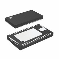
LTC3577EUFF#PBF Linear Technology, LTC3577EUFF#PBF Datasheet - Page 31

LTC3577EUFF#PBF
Manufacturer Part Number
LTC3577EUFF#PBF
Description
IC PWR MANAGEMENT HANDHELD 44QFN
Manufacturer
Linear Technology
Datasheet
1.LTC3577EUFFPBF.pdf
(54 pages)
Specifications of LTC3577EUFF#PBF
Applications
Handheld/Mobile Devices
Voltage - Supply
4.35 V ~ 5.5 V
Operating Temperature
-40°C ~ 85°C
Mounting Type
Surface Mount
Package / Case
44-QFN
Lead Free Status / RoHS Status
Lead free / RoHS Compliant
Current - Supply
-
Available stocks
Company
Part Number
Manufacturer
Quantity
Price
OPERATION
For stability, each LDO output must be bypassed to ground
with a minimum 1μF ceramic capacitor (C
LDO Operating as a Current Limited Switch
The LDO can be used as a current limited switch by simply
connecting the LDOx_FB input to ground. In this case
the LDOx output will be pulled up to V
LDO’s internal current limit (about 300mA). Enabling the
LDO via the I
V
from V
STEP-DOWN SWITCHING REGULATOR OPERATION
Introduction
The LTC3577 includes three 2.25MHz constant frequency
current mode step-down switching regulators providing
500mA, 500mA and 800mA each. All step-down switch-
ing regulators can be programmed for a minimum output
voltage of 0.8V and can be used to power a microcontroller
core, microcontroller I/O, memory or other logic circuitry.
All step-down switching regulators support 100% duty
cycle operation (low dropout mode) when the input volt-
age drops very close to the output voltage and are also
capable of Burst Mode operation for highest effi ciencies
at light loads. Burst Mode operation is individually select-
able for each step-down switching regulator through the
I
step-down switching regulators also include soft-start to
limit inrush current when powering on, short-circuit cur-
rent protection, and switch node slew limiting circuitry
to reduce EMI radiation. No external compensation com-
ponents are required for the switching regulators. The
regulators are sequenced up and down together through
the pushbutton interface (see the “Pushbutton Interface”
section for more information). It is recommended that
the step-down switching regulator input supplies (V
and V
This is recommended because the undervoltage lockout
circuit on the V
down switching regulators when the V
below the V
switching regulator input supplies from a voltage other
than V
2
INLDOx
C register bits BK1BRST, BK2BRST and BK3BRST. The
IN3
OUT
INLDOx
, while disabling the LDO disconnected LDOx
) be connected to the system supply pin (V
the regulators should not be operated outside
OUT
.
2
C interface effectively connects LDOx and
UVLO threshold. If driving the step-down
OUT
pin (V
OUT
UVLO) disables the step-
INLDOx
OUT
OUT
voltage drops
through the
).
OUT
IN12
).
the specifi ed operating range as operation is not guaranteed
beyond this range.
Output Voltage Programming
Figure 13 shows the step-down switching regulator ap-
plication circuit. The full-scale output voltage for each
step-down switching regulator is programmed using a
resistor divider from the step-down switching regulator
output connected to the feedback pins (FB1, FB2 and
FB3) such that:
Typical values for R1 are in the range of 40k to 1M. The
capacitor C
tors and the input capacitance of the FB pin and also helps
to improve transient response for output voltages much
greater than 0.8V. A variety of capacitor sizes can be used
for C
plications. Experimentation with capacitor sizes between
2pF and 22pF may yield improved transient response.
PG_DCDC Operation
The PG_DCDC pin is an open-drain output used to indi-
cate that all step-down switching regulators are enabled
and have reached their fi nal regulation voltage. A 230ms
delay is included from the time all switching regulators
reach 92% of their regulation value to allow a system
controller ample time to reset itself. PG_DCDC may be
used as a power-on reset to a microprocessor powered
by the step-down switching regulators. PG_DCDC is an
Figure 13. Step-Down Switching Regulator Application Circuit
V
EN
MODE
SLEW
OUTx
FB
but a value of 10pF is recommended for most ap-
CONTROL
= 0.8V •
PWM
FB
cancels the pole created by feedback resis-
GND
LTC3577/LTC3577-1
⎛
⎝ ⎜
R2
R1
V
IN
MP
MN
0.8V
+ 1
SWx
FBx
⎞
⎠ ⎟
L
C
FB
R1
R2
3577 F13
C
OUT
31
V
OUTx
3577fa


