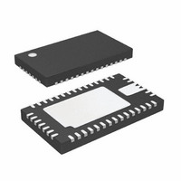
LTC3577EUFF#PBF Linear Technology, LTC3577EUFF#PBF Datasheet - Page 39

LTC3577EUFF#PBF
Manufacturer Part Number
LTC3577EUFF#PBF
Description
IC PWR MANAGEMENT HANDHELD 44QFN
Manufacturer
Linear Technology
Datasheet
1.LTC3577EUFFPBF.pdf
(54 pages)
Specifications of LTC3577EUFF#PBF
Applications
Handheld/Mobile Devices
Voltage - Supply
4.35 V ~ 5.5 V
Operating Temperature
-40°C ~ 85°C
Mounting Type
Surface Mount
Package / Case
44-QFN
Lead Free Status / RoHS Status
Lead free / RoHS Compliant
Current - Supply
-
Available stocks
Company
Part Number
Manufacturer
Quantity
Price
OPERATION
I
The I
to 400kHz. It has built-in timing delays to ensure correct
operation when addressed from an I
device. It also contains input fi lters designed to suppress
glitches should the bus become corrupted.
I
A bus master signals the beginning of communications
by transmitting a START condition. A START condition is
generated by transitioning SDA from HIGH to LOW while
SCL is HIGH. The master may transmit either the slave
write or the slave read address. Once data is written to the
LTC3577, the master may transmit a STOP condition which
commands the LTC3577 to act upon its new command set.
A STOP condition is sent by the master by transitioning
SDA from LOW to HIGH while SCL is HIGH. The bus is
then free for communication with another I
I
Each byte sent to or received from the LTC3577 must
be 8 bits long followed by an extra clock cycle for the
acknowledge bit. The data should be sent to the LTC3577
most signifi cant bit (MSB) fi rst.
SDA
SCL
2
2
2
C Bus Speed
C START and STOP Conditions
C Byte Format
START
2
C port is designed to be operated at speeds of up
0
0
1
0
0
2
SDA
SCL
t
HD, STA
0
0
3
CONDITION
ADDRESS
START
1
1
4
0
0
5
t
LOW
0
0
6
t
r
1
1
7
t
HIGH
t
SU, DAT
WR
0
0
8
2
C compliant master
t
f
ACK
9
A7
1
2
t
C device.
HD, DAT
A6
2
I
A5
2
3
C Timing Diagram
DATA BYTE A
A4
4
REPEATED START
CONDITION
A3
5
I
The acknowledge signal is used for handshaking between
the master and the slave. When the LTC3577 is written
to (write address), it acknowledges its write address as
well as the subsequent two data bytes. When it is read
from (read address), the LTC3577 acknowledges its read
address only. The bus master should acknowledge receipt
of information from the LTC3577.
An acknowledge (active LOW) generated by the LTC3577
lets the master know that the latest byte of information was
received. The acknowledge related clock pulse is generated
by the master. The master releases the SDA line (HIGH)
during the acknowledge clock cycle. The LTC3577 pulls
down the SDA line during the write acknowledge clock
pulse so that it is a stable LOW during the HIGH period
of this clock pulse.
When the LTC3577 is read from, it releases the SDA line so
that the master may acknowledge receipt of the data. Since
the LTC3577 only transmits one byte of data, a master not
acknowledging the data sent by the LTC3577 has no I
specifi c consequence on the operation of the I
2
A2
6
C Acknowledge
t
SU, STA
A1
7
t
HD, STA
A0
t
SP
8
ACK
9
LTC3577/LTC3577-1
B7
1
B6
2
CONDITION
B5
3
STOP
DATA BYTE B
B4
4
t
SU, STO
t
BUF
B3
5
CONDITION
START
B2
6
3577 TD
B1
7
B0
8
ACK
2
9
C port.
39
STOP
3577fa
2
C


