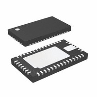
LTC3577EUFF#PBF Linear Technology, LTC3577EUFF#PBF Datasheet - Page 7

LTC3577EUFF#PBF
Manufacturer Part Number
LTC3577EUFF#PBF
Description
IC PWR MANAGEMENT HANDHELD 44QFN
Manufacturer
Linear Technology
Datasheet
1.LTC3577EUFFPBF.pdf
(54 pages)
Specifications of LTC3577EUFF#PBF
Applications
Handheld/Mobile Devices
Voltage - Supply
4.35 V ~ 5.5 V
Operating Temperature
-40°C ~ 85°C
Mounting Type
Surface Mount
Package / Case
44-QFN
Lead Free Status / RoHS Status
Lead free / RoHS Compliant
Current - Supply
-
Available stocks
Company
Part Number
Manufacturer
Quantity
Price
ELECTRICAL CHARACTERISTICS
SYMBOL
R
500mA Step-Down Switching Regulator 2 (Buck2 – Pushbutton Enabled, Second in Sequence)
I
I
V
I
D2
R
R
R
500mA Step-Down Switching Regulator 1 (Buck1 – Pushbutton Enabled, First in Sequence)
I
I
V
I
D1
R
R
R
LDO Regulators.
are at T
SYMBOL
LDO Regulator 1 (LDO1 – Enabled via I
V
V
I
I
I
V
I
I
which apply over the full operating temperature range, otherwise specifi cations are at T
all regulators enabled unless otherwise noted.
VIN12Q
LIM2
FB2
VIN12Q
LIM1
FB1
QLDO1_VO
QLDO1_VI
VINLDO1
LDO1_FB
LDO1_OC
FB2
FB1
INLDO1
OUT_UVLO
LDO1_FB
SW3_PD
P2
N2
SW2_PD
P1
N1
SW1_PD
A
= 25°C. V
PARAMETER
Input Voltage Range
V
V
LD01 V
LD01 V
Shutdown Current
LDO1_FB Regulated Feedback Voltage
LDO1_FB Line Regulation (Note 11)
LDO1_FB Load Regulation (Note 11)
LDO1_FB Input Current
Available Output Current
OUT
OUT
PARAMETER
SW3 Pull-Down in Shutdown
Pulse-Skipping Mode Input Current
Burst Mode Operation Input Current
Shutdown Input Current
Peak PMOS Current Limit
Feedback Voltage
FB2 Input Current
Max Duty Cycle
R
R
SW2 Pull-Down in Shutdown
Pulse-Skipping Mode Input Current
Burst Mode Operation Input Current
Shutdown Input Current
Peak PMOS Current Limit
Feedback Voltage
FB1 Input Current
Max Duty Cycle
R
R
SW1 Pull-Down in Shutdown
DS(ON)
DS(ON)
DS(ON)
DS(ON)
Falling
Rising
INLDO1
OUT
INLDO1
The
of PMOS
of NMOS
of PMOS
of NMOS
Quiescent Current
l
Quiescent Current
= V
denotes the specifi cations which apply over the full operating temperature range, otherwise specifi cations
INLDO2
2
= V
C)
OUT
= V
BAT
= 3.8V, LDO1 and LDO2 enabled unless otherwise noted.
CONDITIONS
POFF State
(Note 10)
(Note 10)
(Note 7)
Pulse-Skipping Mode
Burst Mode Operation
(Note 10)
FB2 = 0V
I
I
POFF State
(Note 10)
(Note 10)
(Note 7)
Pulse-Skipping Mode
Burst Mode Operation
(Note 10)
FB1 = 0V
I
I
POFF State
SW2
SW2
SW1
SW1
CONDITIONS
V
LDO1 is Disabled Below V
LDO1 Enabled, PON State, I
LDO1 Enabled, PON State, I
LDO1 Disabled, PON or POFF State
I
I
I
LDO1_FB = 0.8V
LDO1
LDO1
LDO1
INLDO1
= 100mA
= –100mA
= 100mA
= –100mA
= 1mA
= 1mA, V
= 1mA to 150mA
Step-Down Switching Regulators.
≤ V
OUT
IN
+ 0.3V
= 1.65V to 5.5V
OUT
LDO1
LDO1
UVLO
= 0mA
= 0mA
A
LTC3577/LTC3577-1
= 25°C. V
l
l
l
l
l
l
l
–0.05
–0.05
MIN
0.78
0.78
0.78
0.78
650
100
650
100
1.65
0.78
OUT
MIN
–50
150
2.5
The
= V
l
IN12
denotes the specifi cations
0.01
0.01
TYP
100
900
100
900
0.8
0.8
0.6
0.6
0.8
0.8
0.6
0.6
10
17
10
17
10
0.01
TYP
2.7
2.8
0.1
0.8
0.4
= V
18
5
IN3
= 3.8V,
0.824
0.824
1200
1200
MAX
0.82
0.05
0.82
0.05
MAX
0.82
5.5
2.9
30
50
2
1
UNITS
μV/mA
UNITS
mV/V
3577fa
7
mA
mA
kΩ
kΩ
kΩ
mA
μA
μA
μA
μA
μA
μA
μA
μA
μA
μA
nA
μA
%
%
Ω
Ω
Ω
Ω
V
V
V
V
V
V
V
V


