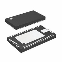
LTC3577EUFF#PBF Linear Technology, LTC3577EUFF#PBF Datasheet - Page 17

LTC3577EUFF#PBF
Manufacturer Part Number
LTC3577EUFF#PBF
Description
IC PWR MANAGEMENT HANDHELD 44QFN
Manufacturer
Linear Technology
Datasheet
1.LTC3577EUFFPBF.pdf
(54 pages)
Specifications of LTC3577EUFF#PBF
Applications
Handheld/Mobile Devices
Voltage - Supply
4.35 V ~ 5.5 V
Operating Temperature
-40°C ~ 85°C
Mounting Type
Surface Mount
Package / Case
44-QFN
Lead Free Status / RoHS Status
Lead free / RoHS Compliant
Current - Supply
-
Available stocks
Company
Part Number
Manufacturer
Quantity
Price
PIN FUNCTIONS
I
This pin is connected to the cathode end of the series LED
backlight string. The current drawn through the series LEDs
can be programmed via a 6-bit 60dB DAC and dimmed via
an internal 4-bit PWM function. I
driver enable, brightness, gradation (soft on/soft off). I
default is LED driver off, current = 0mA.
V
Regulator 1 (LDO1). This pin should be bypassed to ground
with a 1μF or greater ceramic capacitor.
LDO2_FB (Pin 24): Feedback Voltage Input for Low Drop-
out Linear Regulator 2 (LDO2). LDO2 output voltage is
set using an external resistor divider between LDO2 and
LDO2_FB.
FB2 (Pin 25): Feedback Input for Step-Down Switching
Regulator 2 (buck2). This pin servos to a fi xed voltage of
0.8V when the control loop is complete.
FB1 (Pin 26): Feedback Input for Step-Down Switching
Regulator 1 (buck1). This pin servos to a fi xed voltage of
0.8V when the control loop is complete.
LDO1_FB (Pin 27): Feedback Voltage Input for Low Drop-
out Linear Regulator 1 (LDO1). LDO1 output voltage is
set using an external resistor divider between LDO1 and
LDO1_FB.
LDO1 (Pin 28): Output of Low Dropout Linear Regulator 1.
This pin must be bypassed to ground with a 1μF or greater
ceramic capacitor.
LDO2 (Pin 29): Output of Low Dropout Linear Regulator 2.
This pin must be bypassed to ground with a 1μF or greater
ceramic capacitor.
V
Regulator 2 (LDO2). This pin should be bypassed to ground
with a 1μF or greater ceramic capacitor.
SW2 (Pin 31): Power Transmission (Switch) Pin for Step-
Down Switching Regulator 2 (buck2).
V
Regulators 1 and 2. This pin will generally be connected
to V
SW1 (Pin 33): Power Transmission (Switch) Pin for Step-
Down Switching Regulator 1 (buck1).
LED
INLDO1
INLDO2
IN12
OUT
(Pin 22): Series LED Backlight Current Sink Output.
(Pin 32): Power Input for Step-Down Switching
.
(Pin 23): Input Supply of Low Dropout Linear
(Pin 30): Input Supply of Low Dropout Linear
2
C is used to control LED
2
C
NTCBIAS (Pin 34): Output Bias Voltage for NTC. A
resistor from this pin to the NTC pin will bias the NTC
thermistor.
NTC (Pin 35): The NTC pin connects to a battery’s therm-
istor to determine if the battery is too hot or too cold
to charge. If the battery’s temperature is out of range,
charging is paused until it drops back into range. A low
drift bias resistor is required from NTCBIAS to NTC and
a thermistor is required from NTC to ground.
PROG (Pin 36): Charge Current Program and Charge
Current Monitor Pin. Connecting a resistor from PROG
to ground programs the charge current:
If suffi cient input power is available in constant current
mode, this pin servos to 1V. The voltage on this pin always
represents the actual charge current.
IDGATE (Pin 37): Ideal Diode Gate Connection. This
pin controls the gate of an optional external P-channel
MOSFET transistor used to supplement the internal ideal
diode. The source of the P-channel MOSFET should be
connected to V
BAT. It is important to maintain high impedance on this
pin and minimize all leakage paths.
BAT (Pin 38): Single Cell Li-Ion Battery Pin. Depending
on available power and load, a Li-Ion battery on BAT will
either deliver system power to V
diode or be charged from the battery charger.
V
and Input Voltage of the Battery Charger. The majority of
the portable product should be powered from V
LTC3577 will partition the available power between the
external load on V
Priority is given to the external load and any extra power
is used to charge the battery. An ideal diode from BAT to
V
the allotted input current from V
source is removed. V
impedance multilayer ceramic capacitor.
OUT
OUT
I
CHG
(Pin 39): Output Voltage of the PowerPath Controller
ensures that V
=
1000V
R
PROG
OUT
LTC3577/LTC3577-1
( )
OUT
A
OUT
and the drain should be connected to
OUT
is powered even if the load exceeds
and the internal battery charger.
should be bypassed with a low
BUS
OUT
or if the V
through the ideal
BUS
OUT
17
power
. The
3577fa


