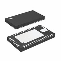
LTC3577EUFF#PBF Linear Technology, LTC3577EUFF#PBF Datasheet - Page 49

LTC3577EUFF#PBF
Manufacturer Part Number
LTC3577EUFF#PBF
Description
IC PWR MANAGEMENT HANDHELD 44QFN
Manufacturer
Linear Technology
Datasheet
1.LTC3577EUFFPBF.pdf
(54 pages)
Specifications of LTC3577EUFF#PBF
Applications
Handheld/Mobile Devices
Voltage - Supply
4.35 V ~ 5.5 V
Operating Temperature
-40°C ~ 85°C
Mounting Type
Surface Mount
Package / Case
44-QFN
Lead Free Status / RoHS Status
Lead free / RoHS Compliant
Current - Supply
-
Available stocks
Company
Part Number
Manufacturer
Quantity
Price
OPERATION
The LTC3557 can be used above 20°C, but the charge
current will be reduced below 1A. The charge current at
a given ambient temperature can be approximated by:
Thus:
Consider the above example with an ambient temperature
of 55°C. The charge current will be reduced to approxi-
mately:
If an external buck switching regulator controlled by the
LTC3577 V
a signifi cant reduction in power dissipated by the LTC3577.
This is because the external buck switching regulator will
drive the PowerPath output (V
battery at 3.3V. If you go through the example above and
substitute 3.6V for V
does not kick in until about 83°C. Thus, the external high
voltage buck regulator not only allows higher charging
currents, but lower power dissipation means a cooler
running application.
Printed Circuit Board Layout
When laying out the printed circuit board, the following
list should be followed to ensure proper operation of the
LTC3577:
1. The Exposed Pad of the package (Pin 45) should connect
directly to a large ground plane to minimize thermal and
electrical impedance.
P
I
I
I
BAT
BAT
BAT
D
=
=
=
=
110°C – T
1.22W – 0.3W
(110°C − T
110°C – 55°C
C
θ
pin is used instead of a 5V wall adapter we see
45°C/W
JA
θ
1.7V
V
5V – 3.3V
JA
OUT
A
= V
A
– BAT
OUT
(
)
− P
OUT
− 0.3W
= 542mA
we see that thermal regulation
DREGS
– BAT
OUT
) to about 3.6V with the
)
•I
BAT
+ P
D(REGS)
2. The step-down switching regulator input supply pins
3. The switching power traces connecting SW1, SW2, and
4. Connections between the step-down switching regu-
5. Keep the buck feedback pin traces (FB1, FB2, and FB3)
6. Connections between the LTC3577 PowerPath pins
7. The boost converter switching power trace connect-
(V
pacitors should be kept as short as possible. The GND
side of these capacitors should connect directly to the
ground plane of the part. These capacitors provide the
AC current to the internal power MOSFETs and their
drivers. It’s important to minimizing inductance from
these capacitors to the pins of the LTC3577. Connect
V
trace.
SW3 to their respective inductors should be minimized
to reduce radiated EMI and parasitic coupling. Due to
the large voltage swing of the switching nodes, sensitive
nodes such as the feedback nodes (FBx, LDOx_FB and
LED_OV) should be kept far away or shielded from the
switching nodes or poor performance could result.
lator inductors and their respective output capacitors
should be kept as short as possible. The GND side of
the output capacitors should connect directly to the
thermal ground plane of the part.
as short as possible. Minimize any parasitic capacitance
between the feedback traces and any switching node
(i.e. SW1, SW2, SW3, and logic signals). If necessary
shield the feedback nodes with a GND trace.
(V
pacitors should be kept as short as possible. The GND
side of these capacitors should connect directly to the
ground plane of the part.
ing SW to the inductor should be minimized to reduce
radiated EMI and parasitic coupling. Due to the large
voltage swing of the SW node, sensitive nodes such
as the feedback nodes (FBx, LDOx_FB and LED_OV)
should be kept far away or shielded from this switching
node or poor performance could result.
IN12
IN12
BUS
and V
and V
and V
IN3
OUT
IN3
LTC3577/LTC3577-1
to V
) and their respective decoupling ca-
) and their respective decoupling ca-
OUT
through a short low impedance
49
3577fa


