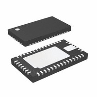
LTC3577EUFF#PBF Linear Technology, LTC3577EUFF#PBF Datasheet - Page 40

LTC3577EUFF#PBF
Manufacturer Part Number
LTC3577EUFF#PBF
Description
IC PWR MANAGEMENT HANDHELD 44QFN
Manufacturer
Linear Technology
Datasheet
1.LTC3577EUFFPBF.pdf
(54 pages)
Specifications of LTC3577EUFF#PBF
Applications
Handheld/Mobile Devices
Voltage - Supply
4.35 V ~ 5.5 V
Operating Temperature
-40°C ~ 85°C
Mounting Type
Surface Mount
Package / Case
44-QFN
Lead Free Status / RoHS Status
Lead free / RoHS Compliant
Current - Supply
-
Available stocks
Company
Part Number
Manufacturer
Quantity
Price
OPERATION
LTC3577/LTC3577-1
I
The LTC3577 responds to a 7-bit address which has been
factory programmed to b’0001001[R/W]’. The LSB of
the address byte, known as the read/write bit, should be
0 when writing data to the LTC3577 and 1 when reading
data from it. Considering the address an eight bit word,
then the write address is 0x12 and the read address is
0x13. The LTC3577 will acknowledge both its read and
write address.
I
The LTC3577 has four command registers for control
input. They are accessed by the I
addressed writing system.
Each write cycle of the LTC3577 consists of exactly three
bytes. The fi rst byte is always the LTC3577’s write address.
The second byte represents the LTC3577’s sub-address.
The sub address is a pointer which directs the subsequent
data byte within the LTC3577. The third byte consists of
the data to be written to the location pointed to by the sub-
address. The LTC3577 contains control registers at only
four sub-address locations: 0x00, 0x01, 0x02 and 0x03.
Writing to sub-addresses outside the four sub-addresses
listed is not recommended as it can cause data in one of
the four listed sub-addresses to be overwritten.
I
The master initiates communication with the LTC3577
with a START condition and the LTC3577’s write address.
If the address matches that of the LTC3577, the LTC3577
returns an acknowledge. The master should then deliver
the sub-address. Again the LTC3577 acknowledges and
the cycle is repeated for the data byte. The data byte is
transferred to an internal holding latch upon the return of
its acknowledge by the LTC3577. This procedure must be
repeated for each sub-address that requires new data. After
one or more cycles of [ADDRESS][SUB-ADDRESS][DATA],
the master may terminate the communication with a STOP
condition. Alternatively, a REPEAT-START condition can be
initiated by the master and another chip on the I
be addressed. This cycle can continue indefi nitely and the
40
2
2
2
C Slave Address
C Sub-Addressed Writing
C Bus Write Operation
2
C port via a sub-
2
C bus can
LTC3577 will remember the last input of valid data that it
received. Once all chips on the bus have been addressed
and sent valid data, a global STOP can be sent and the
LTC3577 will update its command latches with the data
that it had received.
I
The bus master reads the status of the LTC3577 with a
START condition followed by the LTC3577 read address. If
the read address matches that of the LTC3577, the LTC3577
returns an acknowledge. Following the acknowledgement
of its read address the LTC3577 returns one bit of status
information for each of the next 8 clock cycles. A STOP
command is not required for the bus read operation.
I
There are 4 bytes of data that can be written to on the
LTC3577. The bytes are accessed through the sub-
addresses 0x00 to 0x03. At fi rst power application (V
WALL or BAT) all bits default to 0. Additionally all bits are
cleared to 0 when DV
out or if the pushbutton enters the power-down (PDN1
or PDN2) state.
Table 8. LDO and Buck Control Register
Table 8 shows the fi rst byte of data that can be written to
at sub-address 0x00. This byte of data is referred to as
the “LDO and buck control register.”
Bits B0 and B1 enable and disable the LDOs. Writing 1
to B0 or B1 will enable LDO1 or LDO2 respectively, while
writing a 0 will disable the respective LDO.
2
2
LDO and BUCK
CONTROL REGISTER
C Bus Read Operation
C Input Data
BIT
B0
B1
B2
B3
B4
B5
B6
B7
NAME
LDO1EN
LDO2EN
BK1BRST
BK2BRST
BK3BRST
SLEWCTL1
SLEWCTL2
N/A
CC
ADDRESS: 00010010
SUB-ADDRESS: 00000000
FUNCTION
Enable LDO 1
Enable LDO 2
Buck1 Burst Mode Enable
Buck2 Burst Mode Enable
Buck2 Burst Mode Enable
Buck SW Slew Rate: 00 = 1ns,
01 = 2ns, 10 = 4ns, 11 = 8ns
Not Used—No Effect on Operation
drops below its undervoltage lock
BUS
3577fa
,


