MCP215X/40EV-DB Microchip Technology, MCP215X/40EV-DB Datasheet - Page 20
MCP215X/40EV-DB
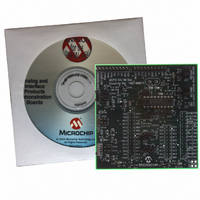
Manufacturer Part Number
MCP215X/40EV-DB
Description
BOARD DEMO FOR MCP215X/40
Manufacturer
Microchip Technology
Datasheet
1.MCP215X40EV-DB.pdf
(94 pages)
Specifications of MCP215X/40EV-DB
Main Purpose
Interface, IrDA
Embedded
Yes, MCU, 8-Bit
Utilized Ic / Part
MCP2150, MCP2155, MCP2140
Primary Attributes
PICDEM™ Demo Board Interface
Processor To Be Evaluated
MCP21x
Interface Type
UART
Lead Free Status / RoHS Status
Contains lead / RoHS non-compliant
Secondary Attributes
-
Lead Free Status / RoHS Status
Lead free / RoHS Compliant, Contains lead / RoHS non-compliant
Available stocks
Company
Part Number
Manufacturer
Quantity
Price
Company:

Part Number:
MCP215X/40EV-DB
Manufacturer:
MICROCHIP
Quantity:
12 000


DS51591A-page 16
Figure 2-3 shows the component layout for the MCP215X/40 Developer’s Daughter
Board and the operation of the JP1, JP2, JP3, JP4 and JP5 jumpers. When the jumper
is open, the signal is pulled high. When the jumper is shorted, the signal is pulled to
ground.
Jumpers JP1 and JP2 are used to specify the MCP215X’s baud rate. The MCP2140
has a fixed baud rate of 9600 baud. The BAUD0 signal is connected to Header H1/H3’s
RB4 pin. The BAUD1 signal is connected to Header H1/H3’s RB5 pin.
Jumpers JP1 and JP2 are used to specify the Host Controller program mode.
The MODE0 signal is connected to Header H1/H3’s RB0 and RA1 pins. The MODE1
signal is connected to Header H1/H3’s RC2 and RE3 pins.
Jumper JP5 are used to specify the MCP215X’s operational state (Enable/Disable).
The MCP2140 has an automatic lower power mode, so is not controlled by a hardware
pin. The EN signal is connected to Header H1/H3’s RB3 pin.
Note:
When using header H3 with the PICDEM FS USB board, refer to Appendix
E. “Using the MCP215X/40 Developer’s Daughter Board with the
PICDEM™ FS USB Demo Board” if the MCP215X/40 Developer’s
Daughter Board PCB is Rev 2.
© 2006 Microchip Technology Inc.
Related parts for MCP215X/40EV-DB
Image
Part Number
Description
Manufacturer
Datasheet
Request
R

Part Number:
Description:
Manufacturer:
Microchip Technology Inc.
Datasheet:
Part Number:
Description:
Manufacturer:
Microchip Technology Inc.
Datasheet:
Part Number:
Description:
Manufacturer:
Microchip Technology Inc.
Datasheet:
Part Number:
Description:
Manufacturer:
Microchip Technology Inc.
Datasheet:
Part Number:
Description:
Manufacturer:
Microchip Technology Inc.
Datasheet:
Part Number:
Description:
Manufacturer:
Microchip Technology Inc.
Datasheet:
Part Number:
Description:
Manufacturer:
Microchip Technology Inc.
Datasheet:
Part Number:
Description:
Manufacturer:
Microchip Technology Inc.
Datasheet: