STEVAL-ISQ002V1 STMicroelectronics, STEVAL-ISQ002V1 Datasheet - Page 158
STEVAL-ISQ002V1
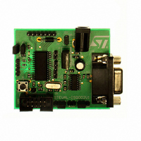
Manufacturer Part Number
STEVAL-ISQ002V1
Description
BOARD EVAL BASED ON ST72264G1
Manufacturer
STMicroelectronics
Specifications of STEVAL-ISQ002V1
Main Purpose
Interface, PMBus
Embedded
Yes, MCU, 8-Bit
Utilized Ic / Part
ST72F264
Primary Attributes
The PMBus™ Interface Using the ST7 I2C Peripheral
Secondary Attributes
Firmware in C Language
Product
Power Management Modules
Lead Free Status / RoHS Status
Lead free / RoHS Compliant
Other names
497-6423
Available stocks
Company
Part Number
Manufacturer
Quantity
Price
Company:

Part Number:
STEVAL-ISQ002V1
Manufacturer:
STMicroelectronics
Quantity:
1


ST72260Gx, ST72262Gx, ST72264Gx
ADC CHARACTERISTICS (Cont’d)
13.12.0.1 General PCB Design Guidelines
To obtain best results, some general design and
layout rules should be followed when designing
the application PCB to shield the noise-sensitive,
analog physical interface from noise generating
CMOS logic signals.
– Properly place components and route the signal
ADC Accuracy with f
Figure 100. ADC Accuracy Characteristics
Notes:
1. ADC Accuracy vs. Negative Injection Current: Injecting negative current on any of the analog input pins significantly
reduces the accuracy of the conversion being performed on another analog input.
For I
for each 10KΩ increase of the external analog source impedance. It is recommended to add a Schottky diode (pin to
ground) to analog pins which may potentially inject negative current. Any positive injection current within the limits spec-
ified for I
2. Refer to
158/172
Symbol
1023
1022
1021
traces on the PCB to shield the analog inputs.
|E
|E
|E
|E
|E
7
6
5
4
3
2
1
INJ-
0
O
G
D
T
L
V
|
|
|
|
|
=0.8mA, the typical leakage induced inside the die is 1.6µA and the effect on the ADC accuracy is a loss of 4 LSB
SS
INJ(PIN)
Digital Result ADCDR
“Typical values” on page 126
1LSB
1
Total unadjusted error
Offset error
Gain Error
Differential linearity error
Integral linearity error
E
O
and ΣI
2
IDEAL
3
Parameter
INJ(PIN)
1)
=
1)
CPU
V
------------------------------- -
4
DD
1024
=8 MHz, f
in
–
5
1 LSB
V
Section 13.8
SS
1)
1)
E
6
T
IDEAL
1)
E
7
L
for more information on typical ADC accuracy values.
ADC
(2)
=4 MHz R
does not affect the ADC accuracy.
Conditions
E
D
1021 1022 1023 1024
(3)
AIN
(1)
< 10
E
G
Analog signals paths should run over the analog
ground plane and be as short as possible. Isolate
analog signals from digital signals that may
switch while the analog inputs are being sampled
by the A/D converter. Do not toggle digital out-
puts on the same I/O port as the A/D input being
converted.
Typ
kΩ,
V
1.5
4
1
1
3
DD
2)
V
FLASH
(1) Example of an actual transfer curve
(2) The ideal transfer curve
(3) End point correlation line
E
between the actual and the ideal transfer curves.
E
transition and the first ideal one.
E
transition and the last actual one.
E
between actual steps and the ideal one.
E
between any actual transition and the end point
correlation line.
DD
T
O
G
D
L
=Total Unadjusted Error: maximum deviation
=Integral Linearity Error: maximum deviation
=Offset Error: deviation between the first actual
=Gain Error: deviation between the last ideal
=Differential Linearity Error: maximum deviation
= 4.5V to 5.5V
V
Max
in
4.5
4.5
4.5
6
5
(LSB
IDEAL
Typ
)
TBD
TBD
TBD
TBD
TBD
2)
ROM
Max
TBD
TBD
TBD
TBD
TBD
Unit
LSB
Related parts for STEVAL-ISQ002V1
Image
Part Number
Description
Manufacturer
Datasheet
Request
R

Part Number:
Description:
BOARD RGB CTR ST7,STP08C596MTR
Manufacturer:
STMicroelectronics
Datasheet:

Part Number:
Description:
Power Management IC Development Tools Full Speed USB to RS232 Bridge Demo
Manufacturer:
STMicroelectronics
Datasheet:
Part Number:
Description:
Power Management IC Development Tools 2.5W solar eval BRD USB SPV1040 LD39050
Manufacturer:
STMicroelectronics
Datasheet:

Part Number:
Description:
BOARD EVAL FOR MEMS SENSORS
Manufacturer:
STMicroelectronics
Datasheet:

Part Number:
Description:
KIT DEV STARTER ST10F276Z5
Manufacturer:
STMicroelectronics
Datasheet:

Part Number:
Description:
BOARD EVAL HDMI $ VIDEO SWITCH
Manufacturer:
STMicroelectronics
Datasheet:

Part Number:
Description:
BOARD DEMO ACCELEROMETER DIL24
Manufacturer:
STMicroelectronics
Datasheet:

Part Number:
Description:
BOARD STLM75/STDS75/ST72F651
Manufacturer:
STMicroelectronics
Datasheet:

Part Number:
Description:
EVAL BOARD 3AXIS MEMS ACCELLRMTR
Manufacturer:
STMicroelectronics
Datasheet:

Part Number:
Description:
BOARD EVAL 8BIT MICRO + TDE1708
Manufacturer:
STMicroelectronics
Datasheet:
Part Number:
Description:
STMicroelectronics [RIPPLE-CARRY BINARY COUNTER/DIVIDERS]
Manufacturer:
STMicroelectronics
Datasheet:
Part Number:
Description:
STMicroelectronics [LIQUID-CRYSTAL DISPLAY DRIVERS]
Manufacturer:
STMicroelectronics
Datasheet:
Part Number:
Description:
BOARD EVAL FOR MEMS SENSORS
Manufacturer:
STMicroelectronics
Datasheet: