STEVAL-PSQ001V1 STMicroelectronics, STEVAL-PSQ001V1 Datasheet - Page 21
STEVAL-PSQ001V1
Manufacturer Part Number
STEVAL-PSQ001V1
Description
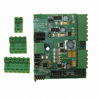
BOARD EVAL BASED ON PM6680A
Manufacturer
STMicroelectronics
Type
Other Power Managementr
Specifications of STEVAL-PSQ001V1
Design Resources
STEVAL-PSQ001V1 Gerber Files STEVAL-PSQ001V1 Schematic STEVAL-PSQ001V1 Bill of Material
Main Purpose
DC/DC, Step Down with LDO
Outputs And Type
6, Non-Isolated
Voltage - Output
0.9 ~ 2.5 V, 1 ~ 3.3 V, 2x 3.3 V, 2.5 V, 5 V
Current - Output
4A, 2A, 800mA, 400mA, 400mA, 150mA
Voltage - Input
5 ~ 36V
Regulator Topology
Buck
Frequency - Switching
200kHz, 300kHz
Board Type
Fully Populated
Utilized Ic / Part
PM6680A
Input Voltage
5 V to 36 V
Output Voltage
1 V to 3.3 V
Product
Power Management Modules
Silicon Manufacturer
ST Micro
Silicon Core Number
PM6680A
Kit Application Type
Power Management
Application Sub Type
Power Supply
Kit Contents
Board
Rohs Compliant
Yes
Lead Free Status / RoHS Status
Lead free / RoHS Compliant
Power - Output
-
Lead Free Status / Rohs Status
Lead free / RoHS Compliant
For Use With/related Products
PM6680A
Other names
497-6425
STEVAL-PSQ001V1
STEVAL-PSQ001V1


PM6680A
7.3
Output ripple compensation and loop stability
In a classic constant on time control, the system regulates the valley value of the output
voltage and not the average value, as shown in
voltage ripple is source of a DC static error.
To compensate this error, an integrator network can be introduced in the control loop, by
connecting the output voltage to the COMP1/COMP2 (for the OUT1 and OUT2 sections
respectively) pin through a capacitor C
Figure 30.
The integrator amplifier generates a current, proportional to the DC errors between the FB
voltage and Vr, which decreases the output voltage in order to compensate the total static
error, including the voltage drop on PCB traces. In addition, C
output ripple. In steady state, the voltage on COMP1/COMP2 pin is the sum of the reference
voltage Vr and the output ripple (see
reaches Vr, a fixed Ton begins and the output increases.
For example, we consider Vout = 5 V with an output ripple of ∆V = 50 mV. Considering C
>> C
an AC path for the output voltage ripple. Then the COMP pin ripple is a replica of the output
ripple, with a DC value of Vr + 25 mV = 925 mV.
For more details about the output ripple compensation network, see the
Closing the integrator loop on page 35
FILT
, the C
Circuitry for output ripple compensation
INT
DC voltage drop VC
Figure
INT
INT
in the Design guidelines.
is about 5 V -Vr + 25 mV = 4.125 V. C
as in
30). In fact when the voltage on the COMP pin
Figure
Figure 28
30.
In this condition, the output
INT
provides an AC path for the
Device description
Chapter 9.6:
INT
assures
21/48
INT
Related parts for STEVAL-PSQ001V1
Image
Part Number
Description
Manufacturer
Datasheet
Request
R

Part Number:
Description:
BOARD ELECT FISCAL CASH REGISTER
Manufacturer:
STMicroelectronics
Datasheet:

Part Number:
Description:
BOARD DEMO LNB PS LNBH23L QFN
Manufacturer:
STMicroelectronics
Datasheet:

Part Number:
Description:
BOARD DEMONSTRATION LNBH PS
Manufacturer:
STMicroelectronics
Datasheet:

Part Number:
Description:
BOARD EVAL FOR MEMS SENSORS
Manufacturer:
STMicroelectronics
Datasheet:
Part Number:
Description:
EVALBOARD/STEVAL-ISV014V1
Manufacturer:
STMicroelectronics
Part Number:
Description:
BOARD EVAL FOR ST802RT1
Manufacturer:
STMicroelectronics
Datasheet:

Part Number:
Description:
BOARD EVAL FOR VACUUM CLEANER
Manufacturer:
STMicroelectronics
Datasheet:

Part Number:
Description:
KIT DEV STARTER ST10F276Z5
Manufacturer:
STMicroelectronics
Datasheet:

Part Number:
Description:
BOARD LED CTLR/DVR STLED316S
Manufacturer:
STMicroelectronics
Datasheet:

Part Number:
Description:
BOARD EVAL BLDC SENSORLESS MOTOR
Manufacturer:
STMicroelectronics
Datasheet:
Part Number:
Description:
STMicroelectronics [RIPPLE-CARRY BINARY COUNTER/DIVIDERS]
Manufacturer:
STMicroelectronics
Datasheet:
Part Number:
Description:
STMicroelectronics [LIQUID-CRYSTAL DISPLAY DRIVERS]
Manufacturer:
STMicroelectronics
Datasheet:
Part Number:
Description:
BOARD EVAL FOR MEMS SENSORS
Manufacturer:
STMicroelectronics
Datasheet: