STEVAL-PSQ001V1 STMicroelectronics, STEVAL-PSQ001V1 Datasheet - Page 30
STEVAL-PSQ001V1
Manufacturer Part Number
STEVAL-PSQ001V1
Description
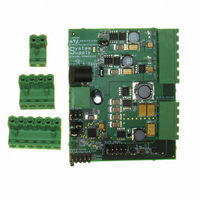
BOARD EVAL BASED ON PM6680A
Manufacturer
STMicroelectronics
Type
Other Power Managementr
Specifications of STEVAL-PSQ001V1
Design Resources
STEVAL-PSQ001V1 Gerber Files STEVAL-PSQ001V1 Schematic STEVAL-PSQ001V1 Bill of Material
Main Purpose
DC/DC, Step Down with LDO
Outputs And Type
6, Non-Isolated
Voltage - Output
0.9 ~ 2.5 V, 1 ~ 3.3 V, 2x 3.3 V, 2.5 V, 5 V
Current - Output
4A, 2A, 800mA, 400mA, 400mA, 150mA
Voltage - Input
5 ~ 36V
Regulator Topology
Buck
Frequency - Switching
200kHz, 300kHz
Board Type
Fully Populated
Utilized Ic / Part
PM6680A
Input Voltage
5 V to 36 V
Output Voltage
1 V to 3.3 V
Product
Power Management Modules
Silicon Manufacturer
ST Micro
Silicon Core Number
PM6680A
Kit Application Type
Power Management
Application Sub Type
Power Supply
Kit Contents
Board
Rohs Compliant
Yes
Lead Free Status / RoHS Status
Lead free / RoHS Compliant
Power - Output
-
Lead Free Status / Rohs Status
Lead free / RoHS Compliant
For Use With/related Products
PM6680A
Other names
497-6425
STEVAL-PSQ001V1
STEVAL-PSQ001V1


Design guidelines
9
9.1
9.2
30/48
Design guidelines
The design of a switching section starts from two parameters:
●
●
Switching frequency
It's possible to set 3 different working frequency ranges for the two sections with FSEL pin
(
Switching frequency mainly influences two parameters:
●
●
Inductor selection
Once that switching frequency is defined, inductor selection depends on the desired
inductor ripple current and load transient performance.
Low inductance means great ripple current and could generate great output noise. On the
other hand, low inductor values involve fast load transient response.
A good compromise between the transient response time, the efficiency, the cost and the
size is to choose the inductor value in order to maintain the inductor ripple current ∆I
between 20 % and 50 % of the maximum output current I
occurs at the maximum input voltage. With this considerations, the inductor value can be
calculated with the following relationship:
Equation 12
where fsw is the switching frequency, V
∆I
In order to prevent overtemperature working conditions, inductor must be able to provide an
RMS current greater than the maximum RMS inductor current I
Equation 13
Where ∆I
Table 6
L
is the selected inductor ripple current.
Input voltage range: in notebook applications it varies from the minimum battery
voltage, VINmin to the AC adapter voltage, V
Maximum load current: it is the maximum required output current, I
Inductor size: for a given saturation current and RMS current, greater frequency allows
to use lower inductor values, which means smaller size.
Efficiency: switching losses are proportional to frequency. High frequency generally
involves low efficiency.
).
L(max)
is the maximum ripple current:
I
LRMS
=
L
I (
=
LOAD
V
IN
f
IN
sw
is the input voltage, V
(max))
−
×
V
∆
OUT
I
L
2
×
INmax
+
V
(
V
OUT
∆
IN
I
.
L
(max))
12
LOAD(max)
OUT
2
LRMS
. The maximum ∆I
is the output voltage and
:
LOAD(max)
.
PM6680A
L
L
Related parts for STEVAL-PSQ001V1
Image
Part Number
Description
Manufacturer
Datasheet
Request
R

Part Number:
Description:
BOARD ELECT FISCAL CASH REGISTER
Manufacturer:
STMicroelectronics
Datasheet:

Part Number:
Description:
BOARD DEMO LNB PS LNBH23L QFN
Manufacturer:
STMicroelectronics
Datasheet:

Part Number:
Description:
BOARD DEMONSTRATION LNBH PS
Manufacturer:
STMicroelectronics
Datasheet:

Part Number:
Description:
BOARD EVAL FOR MEMS SENSORS
Manufacturer:
STMicroelectronics
Datasheet:
Part Number:
Description:
EVALBOARD/STEVAL-ISV014V1
Manufacturer:
STMicroelectronics
Part Number:
Description:
BOARD EVAL FOR ST802RT1
Manufacturer:
STMicroelectronics
Datasheet:

Part Number:
Description:
BOARD EVAL FOR VACUUM CLEANER
Manufacturer:
STMicroelectronics
Datasheet:

Part Number:
Description:
KIT DEV STARTER ST10F276Z5
Manufacturer:
STMicroelectronics
Datasheet:

Part Number:
Description:
BOARD LED CTLR/DVR STLED316S
Manufacturer:
STMicroelectronics
Datasheet:

Part Number:
Description:
BOARD EVAL BLDC SENSORLESS MOTOR
Manufacturer:
STMicroelectronics
Datasheet:
Part Number:
Description:
STMicroelectronics [RIPPLE-CARRY BINARY COUNTER/DIVIDERS]
Manufacturer:
STMicroelectronics
Datasheet:
Part Number:
Description:
STMicroelectronics [LIQUID-CRYSTAL DISPLAY DRIVERS]
Manufacturer:
STMicroelectronics
Datasheet:
Part Number:
Description:
BOARD EVAL FOR MEMS SENSORS
Manufacturer:
STMicroelectronics
Datasheet: