STEVAL-PSQ001V1 STMicroelectronics, STEVAL-PSQ001V1 Datasheet - Page 6
STEVAL-PSQ001V1
Manufacturer Part Number
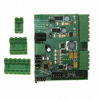
STEVAL-PSQ001V1
Description
BOARD EVAL BASED ON PM6680A
Manufacturer
STMicroelectronics
Type
Other Power Managementr
Specifications of STEVAL-PSQ001V1
Design Resources
STEVAL-PSQ001V1 Gerber Files STEVAL-PSQ001V1 Schematic STEVAL-PSQ001V1 Bill of Material
Main Purpose
DC/DC, Step Down with LDO
Outputs And Type
6, Non-Isolated
Voltage - Output
0.9 ~ 2.5 V, 1 ~ 3.3 V, 2x 3.3 V, 2.5 V, 5 V
Current - Output
4A, 2A, 800mA, 400mA, 400mA, 150mA
Voltage - Input
5 ~ 36V
Regulator Topology
Buck
Frequency - Switching
200kHz, 300kHz
Board Type
Fully Populated
Utilized Ic / Part
PM6680A
Input Voltage
5 V to 36 V
Output Voltage
1 V to 3.3 V
Product
Power Management Modules
Silicon Manufacturer
ST Micro
Silicon Core Number
PM6680A
Kit Application Type
Power Management
Application Sub Type
Power Supply
Kit Contents
Board
Rohs Compliant
Yes
Lead Free Status / RoHS Status
Lead free / RoHS Compliant
Power - Output
-
Lead Free Status / Rohs Status
Lead free / RoHS Compliant
For Use With/related Products
PM6680A
Other names
497-6425
STEVAL-PSQ001V1
STEVAL-PSQ001V1


Pin settings
2.2
6/48
Functions
Table 2.
N°
10
11
12 CSENSE2
13
14
15
16
1
2
3
4
5
6
7
8
9
PHASE2
HGATE2
LGATE2
LGATE1
SGND1
COMP2
SGND2
BOOT2
PGND
SHDN
OUT2
FSEL
EN2
FB2
Pin
NC
Pin functions
Signal ground. Reference for internal logic circuitry. It must be connected to the
signal ground plan of the power supply. The signal ground plan and the power
ground plan must be connected together in one point near the PGND pin.
DC voltage error compensation pin for the switching section 2
Frequency selection pin. It provides a selectable switching frequency, allowing three
different values of switching frequencies for the switching sections.
Enable input for the switching section 2.
• The section 2 is enabled applying a voltage greater than 2.4 V to this pin.
• The section 2 is disabled applying a voltage lower than 0.8 V.
When the section is disabled the High Side gate driver goes low and Low Side gate
driver goes high. If both EN1 and EN2 pins are low and SHDN pin is high the device
enters in standby mode.
Shutdown control input.
• The device switch off if the SHDN voltage is lower than the device off thershold
(Shutdown mode)
• The device switch on if the SHDN voltage is greater than the device on threshold.
The SHDN pin can be connected to the battery through a voltage divider to program
an undervoltage lockout. In shutdown mode, the gate drivers of the two switching
sections are in high impedance (high-Z).
Not connected.
Feedback input for the switching section 2 This pin is connected to a resistive
voltage-divider from OUT2 to PGND to adjust the output voltage from 0.9 V to 3.3 V.
Output voltage sense for the switching section 2.This pin must be directly connected
to the output votage of the switching section.
Bootstrap capacitor connection for the switching section 2. It supplies the high-side
gate driver.
High-side gate driver ouput for section 2. This is the floating gate driver output.
Switch node connection and return path for the high side driver for the section 2.It is
also used as negative current sense input.
Positive current sense input for the switching section 2. This pin must be connected
through a resistor to the drain of the synchronous rectifier (R
a positive current limit threshold for the power supply controller.
Low-side gate driver output for the section 2.
Power ground. This pin must be connected to the power ground plan of the power
supply.
Low-side gate driver output for the section 1.
Signal ground for analog circuitry. It must be connected to the signal ground plan of
the power supply.
Function
DSON
sensing) to obtain
PM6680A
Related parts for STEVAL-PSQ001V1
Image
Part Number
Description
Manufacturer
Datasheet
Request
R

Part Number:
Description:
BOARD ELECT FISCAL CASH REGISTER
Manufacturer:
STMicroelectronics
Datasheet:

Part Number:
Description:
BOARD DEMO LNB PS LNBH23L QFN
Manufacturer:
STMicroelectronics
Datasheet:

Part Number:
Description:
BOARD DEMONSTRATION LNBH PS
Manufacturer:
STMicroelectronics
Datasheet:

Part Number:
Description:
BOARD EVAL FOR MEMS SENSORS
Manufacturer:
STMicroelectronics
Datasheet:
Part Number:
Description:
EVALBOARD/STEVAL-ISV014V1
Manufacturer:
STMicroelectronics
Part Number:
Description:
BOARD EVAL FOR ST802RT1
Manufacturer:
STMicroelectronics
Datasheet:

Part Number:
Description:
BOARD EVAL FOR VACUUM CLEANER
Manufacturer:
STMicroelectronics
Datasheet:

Part Number:
Description:
KIT DEV STARTER ST10F276Z5
Manufacturer:
STMicroelectronics
Datasheet:

Part Number:
Description:
BOARD LED CTLR/DVR STLED316S
Manufacturer:
STMicroelectronics
Datasheet:

Part Number:
Description:
BOARD EVAL BLDC SENSORLESS MOTOR
Manufacturer:
STMicroelectronics
Datasheet:
Part Number:
Description:
STMicroelectronics [RIPPLE-CARRY BINARY COUNTER/DIVIDERS]
Manufacturer:
STMicroelectronics
Datasheet:
Part Number:
Description:
STMicroelectronics [LIQUID-CRYSTAL DISPLAY DRIVERS]
Manufacturer:
STMicroelectronics
Datasheet:
Part Number:
Description:
BOARD EVAL FOR MEMS SENSORS
Manufacturer:
STMicroelectronics
Datasheet: