OM11014 NXP Semiconductors, OM11014 Datasheet - Page 11
OM11014
Manufacturer Part Number
OM11014
Description
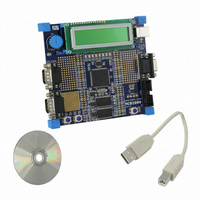
BOARD EVAL FOR LPC2919
Manufacturer
NXP Semiconductors
Series
Keilr
Type
MCUr
Datasheet
1.OM11014.pdf
(67 pages)
Specifications of OM11014
Contents
Board, Cable, CD
For Use With/related Products
LPC2919
Lead Free Status / RoHS Status
Not applicable / Not applicable
Other names
568-4360


NXP Semiconductors
LPC2917_19_1
Product data sheet
7.1.3 IEEE 1149.1 interface pins (JTAG boundary-scan test)
7.1.4 Power supply pins description
7.2.1 Clock architecture
7.2 Clocking strategy
The LPC2917/19 contains boundary-scan test logic according to IEEE 1149.1, also
referred to in this document as JTAG. The boundary-scan test pins can be used to
connect a debugger probe for the embedded ARM processor. Pin JTAGSEL selects
between boundary-scan mode and debug mode.
pins.
Table 5.
Table 6
Table 6.
The LPC2917/19 contains several different internal clock areas. Peripherals like Timers,
SPI, UART, CAN and LIN have their own individual clock sources called Base Clocks. All
base clocks are generated by the Clock Generation Unit (CGU). They may be unrelated in
frequency and phase and can have different clock sources within the CGU.
The system clock for the CPU and AHB Bus infrastructure has its own base clock. This
means most peripherals are clocked independently from the system clock. See
for an overview of the clock areas within the device.
Within each clock area there may be multiple branch clocks, which offers very flexible
control for power-management purposes. All branch clocks are outputs of the Power
Management Unit (PMU) and can be controlled independently. Branch clocks derived
from the same base clock are synchronous in frequency and phase. See
more details of clock and power control within the device.
Symbol
JTAGSEL
TRST_N
TMS
TDI
TDO
TCK
Symbol
V
V
V
V
V
V
V
V
DD(CORE)
SS(CORE)
DD(IO)
SS(IO)
DD(OSC)
SS(OSC)
DDA(ADC3V3)
SS(PLL)
shows the power supply pins.
IEEE 1149.1 boundary-scan test and debug interface
Power supplies
Description
TAP controller select input. LOW-level selects ARM debug mode and HIGH-level
selects boundary scan and flash programming; pulled up internally
test reset input; pulled up internally (active LOW)
test mode select input; pulled up internally
test data input, pulled up internally
test data output
test clock input
Description
digital core supply 1.8 V
digital core ground (digital core, ADC1/2)
I/O pins supply 3.3 V
I/O pins ground
oscillator and PLL supply
oscillator ground
ADC1/2 3.3 V supply
PLL ground
Rev. 01 — 31 July 2008
ARM9 microcontroller with CAN and LIN
Table 5
shows the boundary- scan test
LPC2917/19
© NXP B.V. 2008. All rights reserved.
Section 8.8
Figure 3
11 of 67
for
Related parts for OM11014
Image
Part Number
Description
Manufacturer
Datasheet
Request
R

Part Number:
Description:
NXP Semiconductors designed the LPC2420/2460 microcontroller around a 16-bit/32-bitARM7TDMI-S CPU core with real-time debug interfaces that include both JTAG andembedded trace
Manufacturer:
NXP Semiconductors
Datasheet:

Part Number:
Description:
NXP Semiconductors designed the LPC2458 microcontroller around a 16-bit/32-bitARM7TDMI-S CPU core with real-time debug interfaces that include both JTAG andembedded trace
Manufacturer:
NXP Semiconductors
Datasheet:
Part Number:
Description:
NXP Semiconductors designed the LPC2468 microcontroller around a 16-bit/32-bitARM7TDMI-S CPU core with real-time debug interfaces that include both JTAG andembedded trace
Manufacturer:
NXP Semiconductors
Datasheet:
Part Number:
Description:
NXP Semiconductors designed the LPC2470 microcontroller, powered by theARM7TDMI-S core, to be a highly integrated microcontroller for a wide range ofapplications that require advanced communications and high quality graphic displays
Manufacturer:
NXP Semiconductors
Datasheet:
Part Number:
Description:
NXP Semiconductors designed the LPC2478 microcontroller, powered by theARM7TDMI-S core, to be a highly integrated microcontroller for a wide range ofapplications that require advanced communications and high quality graphic displays
Manufacturer:
NXP Semiconductors
Datasheet:
Part Number:
Description:
The Philips Semiconductors XA (eXtended Architecture) family of 16-bit single-chip microcontrollers is powerful enough to easily handle the requirements of high performance embedded applications, yet inexpensive enough to compete in the market for hi
Manufacturer:
NXP Semiconductors
Datasheet:
Part Number:
Description:
The XA-S3 device is a member of Philips Semiconductors? XA(eXtended Architecture) family of high performance 16-bitsingle-chip microcontrollers
Manufacturer:
NXP Semiconductors
Datasheet:

Part Number:
Description:
The NXP BlueStreak LH75401/LH75411 family consists of two low-cost 16/32-bit System-on-Chip (SoC) devices
Manufacturer:
NXP Semiconductors
Datasheet:
Part Number:
Description:
The NXP LPC3130/3131 combine an 180 MHz ARM926EJ-S CPU core, high-speed USB2
Manufacturer:
NXP Semiconductors
Datasheet:
Part Number:
Description:
The NXP LPC3141 combine a 270 MHz ARM926EJ-S CPU core, High-speed USB 2
Manufacturer:
NXP Semiconductors
Part Number:
Description:
The NXP LPC3143 combine a 270 MHz ARM926EJ-S CPU core, High-speed USB 2
Manufacturer:
NXP Semiconductors

Part Number:
Description:
The NXP LPC3152 combines an 180 MHz ARM926EJ-S CPU core, High-speed USB 2
Manufacturer:
NXP Semiconductors
Part Number:
Description:
The NXP LPC3154 combines an 180 MHz ARM926EJ-S CPU core, High-speed USB 2
Manufacturer:
NXP Semiconductors

Part Number:
Description:
Standard level N-channel enhancement mode Field-Effect Transistor (FET) in a plastic package using NXP High-Performance Automotive (HPA) TrenchMOS technology
Manufacturer:
NXP Semiconductors
Datasheet: