OM11014 NXP Semiconductors, OM11014 Datasheet - Page 28
OM11014
Manufacturer Part Number
OM11014
Description
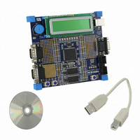
BOARD EVAL FOR LPC2919
Manufacturer
NXP Semiconductors
Series
Keilr
Type
MCUr
Datasheet
1.OM11014.pdf
(67 pages)
Specifications of OM11014
Contents
Board, Cable, CD
For Use With/related Products
LPC2919
Lead Free Status / RoHS Status
Not applicable / Not applicable
Other names
568-4360


NXP Semiconductors
LPC2917_19_1
Product data sheet
8.4.6.1 Overview
8.4.6.2 Description
8.4.6.3 GPIO pin description
8.4.6.4 GPIO clock description
8.4.6 General-purpose I/O
The LPC2917/19 contains four general-purpose I/O ports located at different peripheral
base addresses. In the 144-pin package all four ports are available. All I/O pins are
bidirectional, and the direction can be programmed individually. The I/O pad behavior
depends on the configuration programmed in the port function-select registers.
The key features are:
The general-purpose I/O provides individual control over each bidirectional port pin. There
are two registers to control I/O direction and output level. The inputs are synchronized to
achieve stable read-levels.
To generate an open-drain output, set the bit in the output register to the desired value.
Use the direction register to control the signal. When set to output, the output driver
actively drives the value on the output: when set to input the signal floats and can be
pulled up internally or externally.
The five GPIO ports in the LPC2917/19 have the pins listed below. The GPIO pins are
combined with other functions on the port pins of the LPC2917/19.
GPIO pins.
Table 17.
The GPIO modules are clocked by several clocks, all of which are derived from
BASE_SYS_CLK; CLK_SYS_PESS and CLK_SYS_GPIOx (x = 0-3), see
Note that each GPIO has its own CLK__SYS_GPIOx branch clock for power
management. The frequency of all clocks CLK_SYS_GPIOx is identical to
CLK_SYS_PESS since they are derived from the same base clock BASE_SYS_CLK.
Symbol
GPIO0 pin[31:0]
GPIO1 pin[31:0]
GPIO2 pin[27:0]
GPIO3 pin[15:0]
•
•
•
•
General-purpose parallel inputs and outputs
Direction control of individual bits
Synchronized input sampling for stable input-data values
All I/O defaults to input at reset to avoid any possible bus conflicts
GPIO pins
Direction
IN/OUT
IN/OUT
IN/OUT
IN/OUT
Rev. 01 — 31 July 2008
Description
GPIO port x pins 31 to 0
GPIO port x pins 31 to 0
GPIO port x pins 27 to 0
GPIO port x pins 15 to 0
ARM9 microcontroller with CAN and LIN
LPC2917/19
Table 17
© NXP B.V. 2008. All rights reserved.
Section
shows the
7.2.2.
28 of 67
Related parts for OM11014
Image
Part Number
Description
Manufacturer
Datasheet
Request
R

Part Number:
Description:
NXP Semiconductors designed the LPC2420/2460 microcontroller around a 16-bit/32-bitARM7TDMI-S CPU core with real-time debug interfaces that include both JTAG andembedded trace
Manufacturer:
NXP Semiconductors
Datasheet:

Part Number:
Description:
NXP Semiconductors designed the LPC2458 microcontroller around a 16-bit/32-bitARM7TDMI-S CPU core with real-time debug interfaces that include both JTAG andembedded trace
Manufacturer:
NXP Semiconductors
Datasheet:
Part Number:
Description:
NXP Semiconductors designed the LPC2468 microcontroller around a 16-bit/32-bitARM7TDMI-S CPU core with real-time debug interfaces that include both JTAG andembedded trace
Manufacturer:
NXP Semiconductors
Datasheet:
Part Number:
Description:
NXP Semiconductors designed the LPC2470 microcontroller, powered by theARM7TDMI-S core, to be a highly integrated microcontroller for a wide range ofapplications that require advanced communications and high quality graphic displays
Manufacturer:
NXP Semiconductors
Datasheet:
Part Number:
Description:
NXP Semiconductors designed the LPC2478 microcontroller, powered by theARM7TDMI-S core, to be a highly integrated microcontroller for a wide range ofapplications that require advanced communications and high quality graphic displays
Manufacturer:
NXP Semiconductors
Datasheet:
Part Number:
Description:
The Philips Semiconductors XA (eXtended Architecture) family of 16-bit single-chip microcontrollers is powerful enough to easily handle the requirements of high performance embedded applications, yet inexpensive enough to compete in the market for hi
Manufacturer:
NXP Semiconductors
Datasheet:
Part Number:
Description:
The XA-S3 device is a member of Philips Semiconductors? XA(eXtended Architecture) family of high performance 16-bitsingle-chip microcontrollers
Manufacturer:
NXP Semiconductors
Datasheet:

Part Number:
Description:
The NXP BlueStreak LH75401/LH75411 family consists of two low-cost 16/32-bit System-on-Chip (SoC) devices
Manufacturer:
NXP Semiconductors
Datasheet:
Part Number:
Description:
The NXP LPC3130/3131 combine an 180 MHz ARM926EJ-S CPU core, high-speed USB2
Manufacturer:
NXP Semiconductors
Datasheet:
Part Number:
Description:
The NXP LPC3141 combine a 270 MHz ARM926EJ-S CPU core, High-speed USB 2
Manufacturer:
NXP Semiconductors
Part Number:
Description:
The NXP LPC3143 combine a 270 MHz ARM926EJ-S CPU core, High-speed USB 2
Manufacturer:
NXP Semiconductors

Part Number:
Description:
The NXP LPC3152 combines an 180 MHz ARM926EJ-S CPU core, High-speed USB 2
Manufacturer:
NXP Semiconductors
Part Number:
Description:
The NXP LPC3154 combines an 180 MHz ARM926EJ-S CPU core, High-speed USB 2
Manufacturer:
NXP Semiconductors

Part Number:
Description:
Standard level N-channel enhancement mode Field-Effect Transistor (FET) in a plastic package using NXP High-Performance Automotive (HPA) TrenchMOS technology
Manufacturer:
NXP Semiconductors
Datasheet: