OM11014 NXP Semiconductors, OM11014 Datasheet - Page 14
OM11014
Manufacturer Part Number
OM11014
Description
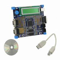
BOARD EVAL FOR LPC2919
Manufacturer
NXP Semiconductors
Series
Keilr
Type
MCUr
Datasheet
1.OM11014.pdf
(67 pages)
Specifications of OM11014
Contents
Board, Cable, CD
For Use With/related Products
LPC2919
Lead Free Status / RoHS Status
Not applicable / Not applicable
Other names
568-4360


NXP Semiconductors
8. Block description
LPC2917_19_1
Product data sheet
8.1.1 Overview
8.1 Flash memory controller
Table 7.
[1]
[2]
[3]
[4]
The Flash Memory Controller (FMC) interfaces to the embedded flash memory for two
tasks:
The flash memory has a 128-bit wide data interface and the flash controller offers two
128-bit buffer lines to improve system performance. The flash has to be programmed
initially via JTAG. In-system programming must be supported by the bootloader.
In-application programming is possible. Flash memory contents can be protected by
disabling JTAG access. Suspension of burning or erasing is not supported.
The key features are:
Base clock
BASE_UART_CLK
BASE_SPI_CLK
BASE_TMR_CLK
BASE_ADC_CLK
BASE_CLK_TESTSHELL
•
•
•
•
•
•
This clock is always on (cannot be switched off for system safety reasons)
In the peripheral subsystem parts of the Timers, watchdog timer, SPI and UART have their own clock
source. See
In the Power Clock and Reset Control subsystem parts of the CGU, RGU PMU have their own clock source.
See
The clock should remain activated when system wake-up on timer or UART is required.
Providing memory data transfer
Memory configuration via triggering, programming and erasing
Programming by CPU via AHB
Programming by external programmer via JTAG
JTAG access protection
Burn-finished and erase-finished interrupt
Section 8.8
Base clock and branch clock overview
Section 8.4
for details.
Rev. 01 — 31 July 2008
for details.
Branch clock name
CLK_UART0
CLK_UART1
CLK_SPI0
CLK_SPI1
CLK_SPI2
CLK_TMR0
CLK_TMR1
CLK_TMR2
CLK_TMR3
CLK_ADC1
CLK_ADC2
CLK_TESTSHELL_IP
ARM9 microcontroller with CAN and LIN
…continued
Parts of the device clocked by
this branch clock
UART 0 interface clock
UART 1 interface clock
SPI 0 interface clock
SPI 1 interface clock
SPI 2 interface clock
Timer 0 clock for counter part
Timer 1 clock for counter part
Timer 2 clock for counter part
Timer 3 clock for counter part
Control of ADC 1, capture sample
result
Control of ADC 2, capture sample
result
LPC2917/19
© NXP B.V. 2008. All rights reserved.
Remark
14 of 67
Related parts for OM11014
Image
Part Number
Description
Manufacturer
Datasheet
Request
R

Part Number:
Description:
NXP Semiconductors designed the LPC2420/2460 microcontroller around a 16-bit/32-bitARM7TDMI-S CPU core with real-time debug interfaces that include both JTAG andembedded trace
Manufacturer:
NXP Semiconductors
Datasheet:

Part Number:
Description:
NXP Semiconductors designed the LPC2458 microcontroller around a 16-bit/32-bitARM7TDMI-S CPU core with real-time debug interfaces that include both JTAG andembedded trace
Manufacturer:
NXP Semiconductors
Datasheet:
Part Number:
Description:
NXP Semiconductors designed the LPC2468 microcontroller around a 16-bit/32-bitARM7TDMI-S CPU core with real-time debug interfaces that include both JTAG andembedded trace
Manufacturer:
NXP Semiconductors
Datasheet:
Part Number:
Description:
NXP Semiconductors designed the LPC2470 microcontroller, powered by theARM7TDMI-S core, to be a highly integrated microcontroller for a wide range ofapplications that require advanced communications and high quality graphic displays
Manufacturer:
NXP Semiconductors
Datasheet:
Part Number:
Description:
NXP Semiconductors designed the LPC2478 microcontroller, powered by theARM7TDMI-S core, to be a highly integrated microcontroller for a wide range ofapplications that require advanced communications and high quality graphic displays
Manufacturer:
NXP Semiconductors
Datasheet:
Part Number:
Description:
The Philips Semiconductors XA (eXtended Architecture) family of 16-bit single-chip microcontrollers is powerful enough to easily handle the requirements of high performance embedded applications, yet inexpensive enough to compete in the market for hi
Manufacturer:
NXP Semiconductors
Datasheet:
Part Number:
Description:
The XA-S3 device is a member of Philips Semiconductors? XA(eXtended Architecture) family of high performance 16-bitsingle-chip microcontrollers
Manufacturer:
NXP Semiconductors
Datasheet:

Part Number:
Description:
The NXP BlueStreak LH75401/LH75411 family consists of two low-cost 16/32-bit System-on-Chip (SoC) devices
Manufacturer:
NXP Semiconductors
Datasheet:
Part Number:
Description:
The NXP LPC3130/3131 combine an 180 MHz ARM926EJ-S CPU core, high-speed USB2
Manufacturer:
NXP Semiconductors
Datasheet:
Part Number:
Description:
The NXP LPC3141 combine a 270 MHz ARM926EJ-S CPU core, High-speed USB 2
Manufacturer:
NXP Semiconductors
Part Number:
Description:
The NXP LPC3143 combine a 270 MHz ARM926EJ-S CPU core, High-speed USB 2
Manufacturer:
NXP Semiconductors

Part Number:
Description:
The NXP LPC3152 combines an 180 MHz ARM926EJ-S CPU core, High-speed USB 2
Manufacturer:
NXP Semiconductors
Part Number:
Description:
The NXP LPC3154 combines an 180 MHz ARM926EJ-S CPU core, High-speed USB 2
Manufacturer:
NXP Semiconductors

Part Number:
Description:
Standard level N-channel enhancement mode Field-Effect Transistor (FET) in a plastic package using NXP High-Performance Automotive (HPA) TrenchMOS technology
Manufacturer:
NXP Semiconductors
Datasheet: