OM11014 NXP Semiconductors, OM11014 Datasheet - Page 32
OM11014
Manufacturer Part Number
OM11014
Description
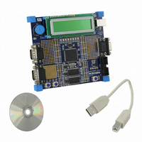
BOARD EVAL FOR LPC2919
Manufacturer
NXP Semiconductors
Series
Keilr
Type
MCUr
Datasheet
1.OM11014.pdf
(67 pages)
Specifications of OM11014
Contents
Board, Cable, CD
For Use With/related Products
LPC2919
Lead Free Status / RoHS Status
Not applicable / Not applicable
Other names
568-4360


NXP Semiconductors
LPC2917_19_1
Product data sheet
Each ADC module has four start inputs. An ADC conversion is started when one of the
start ADC conditions is valid:
The PWM_sync and trans_enable_in of PWM 0 are connected to the 4th match output of
MSCSS timer 0 to start the PWM after a pre-programmed delay. This sync signal is
cascaded through all PWMs, allowing a programmable delay offset between subsequent
PWMs. The sync delay of each PWM can be programmed synchronously or with a
different phase for spreading the power load.
The match outputs of MSCSS timer 1 (PWM control) are connected to the corresponding
carrier inputs of the PWM modules. The carrier signal is modulated with the PWM-
generated waveforms.
The pause input of MSCSS timer 1 (PWM Control) is connected to an external input pin.
Generation of the carrier signal is stopped by asserting the pause of this timer.
The pause input of MSCSS timer 0 (ADC Control) is connected to a ‘NOR’ of the
PWM_sync outputs (start 2 input on the ADCs). If the pause feature of this timer is
enabled the timer only counts when one of the PWM_sync outputs is active HIGH. This
feature can be used to start the ADC once every x PWM cycles, where x corresponds to
the value in the match register of the timer. In this case the start 3 input of the ADC should
be enabled (start on match output of MSCSS timer 0).
The signals connected to the capture inputs of the timers (both MSCSS timer 0 and
MSCSS timer 1) are intended for debugging.
•
•
•
•
Start 0: ADC external start input pin; can be triggered at a positive or negative edge.
Note that this signal is captured in the ADC clock domain
Start 1: If the ‘preceding’ ADC conversion is ended, the sync_out signal starts an ADC
conversion. This signal is captured in the MSCSS subsystem clock domain, see
Section
start 1 input of ADC2 and the sync_out of ADC2 is connected to the start 1 input of
ADC1.
Start 2: The PWM sync_out can start an ADC conversion. The sync_out signal is
synchronized to the ADC clock in the ADC module. This signal is captured in the
MSCSS subsystem clock domain.
Start 3: The match outputs from MSCSS timer 0 are connected to the start 3 inputs of
the ADCs. This signal is captured in the ADC clock domain.
8.7.5.2. As can be seen in
Rev. 01 — 31 July 2008
Figure
8, the sync_out of ADC1 is connected to the
ARM9 microcontroller with CAN and LIN
LPC2917/19
© NXP B.V. 2008. All rights reserved.
32 of 67
Related parts for OM11014
Image
Part Number
Description
Manufacturer
Datasheet
Request
R

Part Number:
Description:
NXP Semiconductors designed the LPC2420/2460 microcontroller around a 16-bit/32-bitARM7TDMI-S CPU core with real-time debug interfaces that include both JTAG andembedded trace
Manufacturer:
NXP Semiconductors
Datasheet:

Part Number:
Description:
NXP Semiconductors designed the LPC2458 microcontroller around a 16-bit/32-bitARM7TDMI-S CPU core with real-time debug interfaces that include both JTAG andembedded trace
Manufacturer:
NXP Semiconductors
Datasheet:
Part Number:
Description:
NXP Semiconductors designed the LPC2468 microcontroller around a 16-bit/32-bitARM7TDMI-S CPU core with real-time debug interfaces that include both JTAG andembedded trace
Manufacturer:
NXP Semiconductors
Datasheet:
Part Number:
Description:
NXP Semiconductors designed the LPC2470 microcontroller, powered by theARM7TDMI-S core, to be a highly integrated microcontroller for a wide range ofapplications that require advanced communications and high quality graphic displays
Manufacturer:
NXP Semiconductors
Datasheet:
Part Number:
Description:
NXP Semiconductors designed the LPC2478 microcontroller, powered by theARM7TDMI-S core, to be a highly integrated microcontroller for a wide range ofapplications that require advanced communications and high quality graphic displays
Manufacturer:
NXP Semiconductors
Datasheet:
Part Number:
Description:
The Philips Semiconductors XA (eXtended Architecture) family of 16-bit single-chip microcontrollers is powerful enough to easily handle the requirements of high performance embedded applications, yet inexpensive enough to compete in the market for hi
Manufacturer:
NXP Semiconductors
Datasheet:
Part Number:
Description:
The XA-S3 device is a member of Philips Semiconductors? XA(eXtended Architecture) family of high performance 16-bitsingle-chip microcontrollers
Manufacturer:
NXP Semiconductors
Datasheet:

Part Number:
Description:
The NXP BlueStreak LH75401/LH75411 family consists of two low-cost 16/32-bit System-on-Chip (SoC) devices
Manufacturer:
NXP Semiconductors
Datasheet:
Part Number:
Description:
The NXP LPC3130/3131 combine an 180 MHz ARM926EJ-S CPU core, high-speed USB2
Manufacturer:
NXP Semiconductors
Datasheet:
Part Number:
Description:
The NXP LPC3141 combine a 270 MHz ARM926EJ-S CPU core, High-speed USB 2
Manufacturer:
NXP Semiconductors
Part Number:
Description:
The NXP LPC3143 combine a 270 MHz ARM926EJ-S CPU core, High-speed USB 2
Manufacturer:
NXP Semiconductors

Part Number:
Description:
The NXP LPC3152 combines an 180 MHz ARM926EJ-S CPU core, High-speed USB 2
Manufacturer:
NXP Semiconductors
Part Number:
Description:
The NXP LPC3154 combines an 180 MHz ARM926EJ-S CPU core, High-speed USB 2
Manufacturer:
NXP Semiconductors

Part Number:
Description:
Standard level N-channel enhancement mode Field-Effect Transistor (FET) in a plastic package using NXP High-Performance Automotive (HPA) TrenchMOS technology
Manufacturer:
NXP Semiconductors
Datasheet: