C8051F300DK Silicon Laboratories Inc, C8051F300DK Datasheet - Page 105
C8051F300DK
Manufacturer Part Number
C8051F300DK
Description
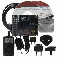
DEV KIT F300/301/302/303/304/305
Manufacturer
Silicon Laboratories Inc
Type
MCUr
Specifications of C8051F300DK
Contents
Evaluation Board, Power Supply, USB Cables, Adapter and Documentation
Processor To Be Evaluated
C8051F30x
Interface Type
USB
Silicon Manufacturer
Silicon Labs
Core Architecture
8051
Silicon Core Number
C8051F300
Silicon Family Name
C8051F30x
Lead Free Status / RoHS Status
Contains lead / RoHS non-compliant
For Use With/related Products
Silicon Laboratories C8051 F300/001/002
Lead Free Status / Rohs Status
Lead free / RoHS Compliant
Other names
336-1246


Registers XBR1 and XBR2 are used to assign the digital I/O resources to the physical I/O Port pins. Note
that when the SMBus is selected, the Crossbar assigns both pins associated with the SMBus (SDA and
SCL). Either or both of the UART signals may be selected by the Crossbar. UART0 pin assignments are
fixed for bootloading purposes: when UART TX0 is selected, it is always assigned to P0.4; when UART
RX0 is selected, it is always assigned to P0.5. Standard Port I/Os appear contiguously after the prioritized
functions have been assigned. For example, if assigned functions that take the first 3 Port I/O (P0.[2:0]), 5
Port I/O are left for analog or GPIO use.
SF Signals
PIN I/O
TX0
RX0
SDA
SCL
CP0
CP0A
SYSCLK
CEX0
CEX1
CEX2
ECI
T0
T1
SF Signals
Figure 12.4. Crossbar Priority Decoder with XBR0 = 0x44
VREF
0
0
Port pin potentially available to peripheral
Port pin skipped by CrossBar
Special Function Signals are not assigned by the crossbar. When
these signals are enabled, the CrossBar must be manually
configured to skip their corresponding port pins. Note: x1 refers to
the XTAL1 signal; x2 refers to the XTAL2 signal.
1
0
x1
2
1
XBR0[0:7]
x2
3
0
P0
4
0
Rev. 2.9
5
0
CNVSTR
6
1
7
0
C8051F300/1/2/3/4/5
105
Related parts for C8051F300DK
Image
Part Number
Description
Manufacturer
Datasheet
Request
R

Part Number:
Description:
SMD/C°/SINGLE-ENDED OUTPUT SILICON OSCILLATOR
Manufacturer:
Silicon Laboratories Inc
Part Number:
Description:
Manufacturer:
Silicon Laboratories Inc
Datasheet:
Part Number:
Description:
N/A N/A/SI4010 AES KEYFOB DEMO WITH LCD RX
Manufacturer:
Silicon Laboratories Inc
Datasheet:
Part Number:
Description:
N/A N/A/SI4010 SIMPLIFIED KEY FOB DEMO WITH LED RX
Manufacturer:
Silicon Laboratories Inc
Datasheet:
Part Number:
Description:
N/A/-40 TO 85 OC/EZLINK MODULE; F930/4432 HIGH BAND (REV E/B1)
Manufacturer:
Silicon Laboratories Inc
Part Number:
Description:
EZLink Module; F930/4432 Low Band (rev e/B1)
Manufacturer:
Silicon Laboratories Inc
Part Number:
Description:
I°/4460 10 DBM RADIO TEST CARD 434 MHZ
Manufacturer:
Silicon Laboratories Inc
Part Number:
Description:
I°/4461 14 DBM RADIO TEST CARD 868 MHZ
Manufacturer:
Silicon Laboratories Inc
Part Number:
Description:
I°/4463 20 DBM RFSWITCH RADIO TEST CARD 460 MHZ
Manufacturer:
Silicon Laboratories Inc
Part Number:
Description:
I°/4463 20 DBM RADIO TEST CARD 868 MHZ
Manufacturer:
Silicon Laboratories Inc
Part Number:
Description:
I°/4463 27 DBM RADIO TEST CARD 868 MHZ
Manufacturer:
Silicon Laboratories Inc
Part Number:
Description:
I°/4463 SKYWORKS 30 DBM RADIO TEST CARD 915 MHZ
Manufacturer:
Silicon Laboratories Inc
Part Number:
Description:
N/A N/A/-40 TO 85 OC/4463 RFMD 30 DBM RADIO TEST CARD 915 MHZ
Manufacturer:
Silicon Laboratories Inc
Part Number:
Description:
I°/4463 20 DBM RADIO TEST CARD 169 MHZ
Manufacturer:
Silicon Laboratories Inc