C8051F300DK Silicon Laboratories Inc, C8051F300DK Datasheet - Page 4
C8051F300DK
Manufacturer Part Number
C8051F300DK
Description
DEV KIT F300/301/302/303/304/305
Manufacturer
Silicon Laboratories Inc
Type
MCUr
Specifications of C8051F300DK
Contents
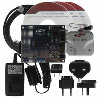
Evaluation Board, Power Supply, USB Cables, Adapter and Documentation
Processor To Be Evaluated
C8051F30x
Interface Type
USB
Silicon Manufacturer
Silicon Labs
Core Architecture
8051
Silicon Core Number
C8051F300
Silicon Family Name
C8051F30x
Lead Free Status / RoHS Status
Contains lead / RoHS non-compliant
For Use With/related Products
Silicon Laboratories C8051 F300/001/002
Lead Free Status / Rohs Status
Lead free / RoHS Compliant
Other names
336-1246


C8051F300/1/2/3/4/5
9. Reset Sources......................................................................................................... 83
10. Flash Memory ......................................................................................................... 89
11. Oscillators ............................................................................................................... 97
12. Port Input/Output.................................................................................................. 103
13. SMBus ................................................................................................................... 111
4
8.4. Power Management Modes .............................................................................. 80
9.1. Power-On Reset ............................................................................................... 84
9.2. Power-Fail Reset/VDD Monitor......................................................................... 84
9.3. External Reset .................................................................................................. 85
9.4. Missing Clock Detector Reset........................................................................... 85
9.5. Comparator0 Reset........................................................................................... 85
9.6. PCA Watchdog Timer Reset............................................................................. 85
9.7. Flash Error Reset.............................................................................................. 86
9.8. Software Reset ................................................................................................. 86
10.1.Programming The Flash Memory ..................................................................... 89
10.2.Non-Volatile Data Storage................................................................................ 90
10.3.Security Options ............................................................................................... 90
10.4.Flash Write and Erase Guidelines .................................................................... 94
11.1.Programmable Internal Oscillator ..................................................................... 97
11.2.External Oscillator Drive Circuit........................................................................ 99
11.3.System Clock Selection.................................................................................... 99
11.4.External Crystal Example ............................................................................... 101
11.5.External RC Example ..................................................................................... 102
11.6.External Capacitor Example ........................................................................... 102
12.1.Priority Crossbar Decoder .............................................................................. 104
12.2.Port I/O Initialization ....................................................................................... 106
12.3.General Purpose Port I/O ............................................................................... 108
13.1.Supporting Documents ................................................................................... 112
13.2.SMBus Configuration...................................................................................... 112
13.3.SMBus Operation ........................................................................................... 112
8.3.4. Interrupt Latency ...................................................................................... 73
8.3.5. Interrupt Register Descriptions................................................................. 75
8.4.1. Idle Mode.................................................................................................. 80
8.4.2. Stop Mode ................................................................................................ 81
10.1.1.Flash Lock and Key Functions ................................................................. 89
10.1.2.Flash Erase Procedure ............................................................................ 89
10.1.3.Flash Write Procedure ............................................................................. 90
10.4.1.V
10.4.2.PSWE Maintenance ................................................................................. 94
10.4.3.System Clock ........................................................................................... 95
13.3.1.Arbitration............................................................................................... 113
13.3.2.Clock Low Extension.............................................................................. 114
13.3.3.SCL Low Timeout................................................................................... 114
13.3.4.SCL High (SMBus Free) Timeout .......................................................... 114
DD
Maintenance and the V
Rev. 2.9
DD
monitor ................................................... 94
Related parts for C8051F300DK
Image
Part Number
Description
Manufacturer
Datasheet
Request
R

Part Number:
Description:
SMD/C°/SINGLE-ENDED OUTPUT SILICON OSCILLATOR
Manufacturer:
Silicon Laboratories Inc
Part Number:
Description:
Manufacturer:
Silicon Laboratories Inc
Datasheet:
Part Number:
Description:
N/A N/A/SI4010 AES KEYFOB DEMO WITH LCD RX
Manufacturer:
Silicon Laboratories Inc
Datasheet:
Part Number:
Description:
N/A N/A/SI4010 SIMPLIFIED KEY FOB DEMO WITH LED RX
Manufacturer:
Silicon Laboratories Inc
Datasheet:
Part Number:
Description:
N/A/-40 TO 85 OC/EZLINK MODULE; F930/4432 HIGH BAND (REV E/B1)
Manufacturer:
Silicon Laboratories Inc
Part Number:
Description:
EZLink Module; F930/4432 Low Band (rev e/B1)
Manufacturer:
Silicon Laboratories Inc
Part Number:
Description:
I°/4460 10 DBM RADIO TEST CARD 434 MHZ
Manufacturer:
Silicon Laboratories Inc
Part Number:
Description:
I°/4461 14 DBM RADIO TEST CARD 868 MHZ
Manufacturer:
Silicon Laboratories Inc
Part Number:
Description:
I°/4463 20 DBM RFSWITCH RADIO TEST CARD 460 MHZ
Manufacturer:
Silicon Laboratories Inc
Part Number:
Description:
I°/4463 20 DBM RADIO TEST CARD 868 MHZ
Manufacturer:
Silicon Laboratories Inc
Part Number:
Description:
I°/4463 27 DBM RADIO TEST CARD 868 MHZ
Manufacturer:
Silicon Laboratories Inc
Part Number:
Description:
I°/4463 SKYWORKS 30 DBM RADIO TEST CARD 915 MHZ
Manufacturer:
Silicon Laboratories Inc
Part Number:
Description:
N/A N/A/-40 TO 85 OC/4463 RFMD 30 DBM RADIO TEST CARD 915 MHZ
Manufacturer:
Silicon Laboratories Inc
Part Number:
Description:
I°/4463 20 DBM RADIO TEST CARD 169 MHZ
Manufacturer:
Silicon Laboratories Inc