C8051F300DK Silicon Laboratories Inc, C8051F300DK Datasheet - Page 26
C8051F300DK
Manufacturer Part Number
C8051F300DK
Description
DEV KIT F300/301/302/303/304/305
Manufacturer
Silicon Laboratories Inc
Type
MCUr
Specifications of C8051F300DK
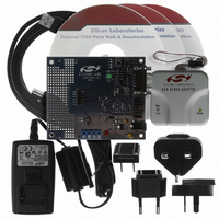
Contents
Evaluation Board, Power Supply, USB Cables, Adapter and Documentation
Processor To Be Evaluated
C8051F30x
Interface Type
USB
Silicon Manufacturer
Silicon Labs
Core Architecture
8051
Silicon Core Number
C8051F300
Silicon Family Name
C8051F30x
Lead Free Status / RoHS Status
Contains lead / RoHS non-compliant
For Use With/related Products
Silicon Laboratories C8051 F300/001/002
Lead Free Status / Rohs Status
Lead free / RoHS Compliant
Other names
336-1246


C8051F300/1/2/3/4/5
Table 3.1. Global Electrical Characteristics (Continued)
–40 to +85 °C, 25 MHz system clock unless otherwise specified.
26
I
I
(Note 3, Note 5)
Digital Supply Current
(Stop Mode, shutdown)
Notes:
DD
DD
1. Given in Table 9.2 on page 86.
2. SYSCLK must be at least 32 kHz to enable debugging.
3. Based on device characterization data; Not production tested.
4. Normal IDD can be estimated for frequencies <= 15 MHz by simply multiplying the frequency of interest by
5. Idle IDD can be estimated for frequencies <= 1 MHz by simply multiplying the frequency of interest by the
Supply Sensitivity (Note 3) F = 25 MHz
Frequency Sensitivity
the frequency sensitivity number for that range. When using these numbers to estimate I
estimate should be the current at 25 MHz minus the difference in current indicated by the frequency sensitivity
number.
For example: V
frequency sensitivity number for that range. When using these numbers to estimate Idle I
estimate should be the current at 25 MHz minus the difference in current indicated by the frequency sensitivity
number.
For example: V
Parameter
DD
DD
= 3.0 V; F = 20 MHz, I
= 3.0 V; F = 5 MHz, Idle I
F = 1 MHz
V
V
V
V
Oscillator not running,
V
DD
DD
DD
DD
DD
= 3.0 V, F <= 1 MHz, T = 25
= 3.0 V, F > 1 MHz, T = 25
= 3.6 V, F <= 1 MHz, T = 25
= 3.6 V, F > 1 MHz, T = 25
Monitor Disabled
DD
Conditions
DD
= 6.6 mA – (25 MHz – 20 MHz) x 0.16 mA/MHz = 5.8 mA.
Rev. 2.9
= 3.3 mA – (25 MHz – 5 MHz) x 0.10 mA/MHz = 1.3 mA.
°
°
C
C
°
°
C
C
Min
—
—
—
—
—
—
—
< 0.1
0.27
0.10
0.35
0.12
Typ
47
59
DD
DD
Max
for >15 MHz, the
for >1 MHz, the
—
—
—
—
—
—
—
mA/MHz
mA/MHz
mA/MHz
mA/MHz
Units
%/V
%/V
µA
Related parts for C8051F300DK
Image
Part Number
Description
Manufacturer
Datasheet
Request
R

Part Number:
Description:
SMD/C°/SINGLE-ENDED OUTPUT SILICON OSCILLATOR
Manufacturer:
Silicon Laboratories Inc
Part Number:
Description:
Manufacturer:
Silicon Laboratories Inc
Datasheet:
Part Number:
Description:
N/A N/A/SI4010 AES KEYFOB DEMO WITH LCD RX
Manufacturer:
Silicon Laboratories Inc
Datasheet:
Part Number:
Description:
N/A N/A/SI4010 SIMPLIFIED KEY FOB DEMO WITH LED RX
Manufacturer:
Silicon Laboratories Inc
Datasheet:
Part Number:
Description:
N/A/-40 TO 85 OC/EZLINK MODULE; F930/4432 HIGH BAND (REV E/B1)
Manufacturer:
Silicon Laboratories Inc
Part Number:
Description:
EZLink Module; F930/4432 Low Band (rev e/B1)
Manufacturer:
Silicon Laboratories Inc
Part Number:
Description:
I°/4460 10 DBM RADIO TEST CARD 434 MHZ
Manufacturer:
Silicon Laboratories Inc
Part Number:
Description:
I°/4461 14 DBM RADIO TEST CARD 868 MHZ
Manufacturer:
Silicon Laboratories Inc
Part Number:
Description:
I°/4463 20 DBM RFSWITCH RADIO TEST CARD 460 MHZ
Manufacturer:
Silicon Laboratories Inc
Part Number:
Description:
I°/4463 20 DBM RADIO TEST CARD 868 MHZ
Manufacturer:
Silicon Laboratories Inc
Part Number:
Description:
I°/4463 27 DBM RADIO TEST CARD 868 MHZ
Manufacturer:
Silicon Laboratories Inc
Part Number:
Description:
I°/4463 SKYWORKS 30 DBM RADIO TEST CARD 915 MHZ
Manufacturer:
Silicon Laboratories Inc
Part Number:
Description:
N/A N/A/-40 TO 85 OC/4463 RFMD 30 DBM RADIO TEST CARD 915 MHZ
Manufacturer:
Silicon Laboratories Inc
Part Number:
Description:
I°/4463 20 DBM RADIO TEST CARD 169 MHZ
Manufacturer:
Silicon Laboratories Inc