C8051F300DK Silicon Laboratories Inc, C8051F300DK Datasheet - Page 52
C8051F300DK
Manufacturer Part Number
C8051F300DK
Description
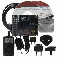
DEV KIT F300/301/302/303/304/305
Manufacturer
Silicon Laboratories Inc
Type
MCUr
Specifications of C8051F300DK
Contents
Evaluation Board, Power Supply, USB Cables, Adapter and Documentation
Processor To Be Evaluated
C8051F30x
Interface Type
USB
Silicon Manufacturer
Silicon Labs
Core Architecture
8051
Silicon Core Number
C8051F300
Silicon Family Name
C8051F30x
Lead Free Status / RoHS Status
Contains lead / RoHS non-compliant
For Use With/related Products
Silicon Laboratories C8051 F300/001/002
Lead Free Status / Rohs Status
Lead free / RoHS Compliant
Other names
336-1246


C8051F300/1/2/3/4/5
The output of Comparator0 can be polled in software, used as an interrupt source, and/or routed to a Port
pin. When routed to a Port pin, the Comparator0 output is available asynchronous or synchronous to the
system clock; the asynchronous output is available even in STOP mode (with no system clock active).
When disabled, the Comparator0 output (if assigned to a Port I/O pin via the Crossbar) defaults to the logic
low state, and its supply current falls to less than 100 nA. See
Decoder” on page 104
Comparator0 inputs can be externally driven from –0.25 to (V
complete electrical specifications for Comparator0 are given in Table 7.1.
The Comparator0 response time may be configured in software via the CP0MD1-0 bits in register
CPT0MD (see SFR Definition 7.3). Selecting a longer response time reduces the amount of power con-
sumed by Comparator0. See Table 7.1 for complete timing and power consumption specifications.
The hysteresis of Comparator0 is software-programmable via its Comparator0 Control register (CPT0CN).
The user can program both the amount of hysteresis voltage (referred to the input voltage) and the positive
and negative-going symmetry of this hysteresis around the threshold voltage.
The Comparator0 hysteresis is programmed using Bits3–0 in the Comparator0 Control Register CPT0CN
(shown in SFR Definition 7.1). The amount of negative hysteresis voltage is determined by the settings of
the CP0HYN bits. As shown in Figure 7.2, settings of 20, 10 or 5 mV of negative hysteresis can be pro-
grammed, or negative hysteresis can be disabled. In a similar way, the amount of positive hysteresis is
determined by the setting the CP0HYP bits.
52
(Programmed with CP0HYP Bits)
Positive Hysteresis Voltage
INPUTS
OUTPUT
VIN+
VIN-
CIRCUIT CONFIGURATION
Positive Hysteresis
CP0-
CP0+
VIN+
VIN-
Disabled
V
for details on configuring the Comparator0 output via the digital Crossbar.
OL
Figure 7.2. Comparator Hysteresis Plot
V
OH
+
_
CP0
Positive Hysteresis
Maximum
OUT
Rev. 2.9
Negative Hysteresis
Disabled
DD
) + 0.25 V without damage or upset. The
Section “12.1. Priority Crossbar
Negative Hysteresis
(Programmed by CP0HYN Bits)
Maximum
Negative Hysteresis Voltage
Related parts for C8051F300DK
Image
Part Number
Description
Manufacturer
Datasheet
Request
R

Part Number:
Description:
SMD/C°/SINGLE-ENDED OUTPUT SILICON OSCILLATOR
Manufacturer:
Silicon Laboratories Inc
Part Number:
Description:
Manufacturer:
Silicon Laboratories Inc
Datasheet:
Part Number:
Description:
N/A N/A/SI4010 AES KEYFOB DEMO WITH LCD RX
Manufacturer:
Silicon Laboratories Inc
Datasheet:
Part Number:
Description:
N/A N/A/SI4010 SIMPLIFIED KEY FOB DEMO WITH LED RX
Manufacturer:
Silicon Laboratories Inc
Datasheet:
Part Number:
Description:
N/A/-40 TO 85 OC/EZLINK MODULE; F930/4432 HIGH BAND (REV E/B1)
Manufacturer:
Silicon Laboratories Inc
Part Number:
Description:
EZLink Module; F930/4432 Low Band (rev e/B1)
Manufacturer:
Silicon Laboratories Inc
Part Number:
Description:
I°/4460 10 DBM RADIO TEST CARD 434 MHZ
Manufacturer:
Silicon Laboratories Inc
Part Number:
Description:
I°/4461 14 DBM RADIO TEST CARD 868 MHZ
Manufacturer:
Silicon Laboratories Inc
Part Number:
Description:
I°/4463 20 DBM RFSWITCH RADIO TEST CARD 460 MHZ
Manufacturer:
Silicon Laboratories Inc
Part Number:
Description:
I°/4463 20 DBM RADIO TEST CARD 868 MHZ
Manufacturer:
Silicon Laboratories Inc
Part Number:
Description:
I°/4463 27 DBM RADIO TEST CARD 868 MHZ
Manufacturer:
Silicon Laboratories Inc
Part Number:
Description:
I°/4463 SKYWORKS 30 DBM RADIO TEST CARD 915 MHZ
Manufacturer:
Silicon Laboratories Inc
Part Number:
Description:
N/A N/A/-40 TO 85 OC/4463 RFMD 30 DBM RADIO TEST CARD 915 MHZ
Manufacturer:
Silicon Laboratories Inc
Part Number:
Description:
I°/4463 20 DBM RADIO TEST CARD 169 MHZ
Manufacturer:
Silicon Laboratories Inc