C8051F300DK Silicon Laboratories Inc, C8051F300DK Datasheet - Page 91
C8051F300DK
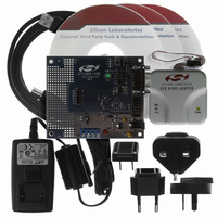
Manufacturer Part Number
C8051F300DK
Description
DEV KIT F300/301/302/303/304/305
Manufacturer
Silicon Laboratories Inc
Type
MCUr
Specifications of C8051F300DK
Contents
Evaluation Board, Power Supply, USB Cables, Adapter and Documentation
Processor To Be Evaluated
C8051F30x
Interface Type
USB
Silicon Manufacturer
Silicon Labs
Core Architecture
8051
Silicon Core Number
C8051F300
Silicon Family Name
C8051F30x
Lead Free Status / RoHS Status
Contains lead / RoHS non-compliant
For Use With/related Products
Silicon Laboratories C8051 F300/001/002
Lead Free Status / Rohs Status
Lead free / RoHS Compliant
Other names
336-1246


The lock bits can always be read and cleared to logic 0 regardless of the security settings.
Important note: The only means of removing a lock (write or read/write) once set is to erase the
entire program memory space via a C2 Device Erase command.
The level of Flash security depends on the Flash access method. The three Flash access methods that
can be restricted are reads, writes, and erases from the C2 debug interface, user firmware executing on
unlocked pages, and user firmware executing on locked pages.
Accessing Flash from the C2 debug interface:
1. Any unlocked page may be read, written, or erased.
2. Locked pages cannot be read, written, or erased.
3. The page containing the Lock Byte may be read, written, or erased if it is unlocked.
4. Reading the contents of the Lock Byte is always permitted only if no pages are locked.
5. Locking additional pages (changing ‘1’s to ‘0’s in the Lock Byte) is not permitted.
6. Unlocking Flash pages (changing ‘0’s to ‘1’s in the Lock Byte) requires the C2 Device Erase com-
7. The Reserved Area cannot be read, written, or erased.
organized in 512-byte
mand, which erases all Flash pages including the page containing the Lock Byte and the Lock
Byte itself.
C8051F300/1/2/3
FLASH memory
Lock Byte
Reserved
pages
Bits
7–4
3–0
Figure 10.1. Flash Program Memory Map
0x1E00
0x1DFF
0x1DFE
0x0000
Write Lock: Clearing any of these bits to logic 0 prevents all Flash
memory from being written or page-erased across the C2 interface
Read/Write Lock: Clearing any of these bits to logic 0 prevents all
Flash memory from being read, written, or page-erased across the
C2 interface.
Table 10.2. Security Byte Decoding
organized in 512-byte
FLASH memory
C8051F304
Lock Byte
Reserved
pages
Rev. 2.9
Description
0x1000
0x0FFF
0x0FFE
0x0000
C8051F300/1/2/3/4/5
organized in 512-byte
FLASH memory
C8051F305
Lock Byte
Reserved
pages
0x0800
0x07FF
0x07FE
0x0000
91
Related parts for C8051F300DK
Image
Part Number
Description
Manufacturer
Datasheet
Request
R

Part Number:
Description:
SMD/C°/SINGLE-ENDED OUTPUT SILICON OSCILLATOR
Manufacturer:
Silicon Laboratories Inc
Part Number:
Description:
Manufacturer:
Silicon Laboratories Inc
Datasheet:
Part Number:
Description:
N/A N/A/SI4010 AES KEYFOB DEMO WITH LCD RX
Manufacturer:
Silicon Laboratories Inc
Datasheet:
Part Number:
Description:
N/A N/A/SI4010 SIMPLIFIED KEY FOB DEMO WITH LED RX
Manufacturer:
Silicon Laboratories Inc
Datasheet:
Part Number:
Description:
N/A/-40 TO 85 OC/EZLINK MODULE; F930/4432 HIGH BAND (REV E/B1)
Manufacturer:
Silicon Laboratories Inc
Part Number:
Description:
EZLink Module; F930/4432 Low Band (rev e/B1)
Manufacturer:
Silicon Laboratories Inc
Part Number:
Description:
I°/4460 10 DBM RADIO TEST CARD 434 MHZ
Manufacturer:
Silicon Laboratories Inc
Part Number:
Description:
I°/4461 14 DBM RADIO TEST CARD 868 MHZ
Manufacturer:
Silicon Laboratories Inc
Part Number:
Description:
I°/4463 20 DBM RFSWITCH RADIO TEST CARD 460 MHZ
Manufacturer:
Silicon Laboratories Inc
Part Number:
Description:
I°/4463 20 DBM RADIO TEST CARD 868 MHZ
Manufacturer:
Silicon Laboratories Inc
Part Number:
Description:
I°/4463 27 DBM RADIO TEST CARD 868 MHZ
Manufacturer:
Silicon Laboratories Inc
Part Number:
Description:
I°/4463 SKYWORKS 30 DBM RADIO TEST CARD 915 MHZ
Manufacturer:
Silicon Laboratories Inc
Part Number:
Description:
N/A N/A/-40 TO 85 OC/4463 RFMD 30 DBM RADIO TEST CARD 915 MHZ
Manufacturer:
Silicon Laboratories Inc
Part Number:
Description:
I°/4463 20 DBM RADIO TEST CARD 169 MHZ
Manufacturer:
Silicon Laboratories Inc