C8051F996DK Silicon Laboratories Inc, C8051F996DK Datasheet - Page 32
C8051F996DK
Manufacturer Part Number
C8051F996DK
Description
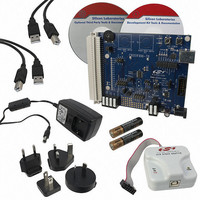
KIT DEV FOR C8051F996
Manufacturer
Silicon Laboratories Inc
Type
MCUr
Datasheets
1.C8051F996DK.pdf
(24 pages)
2.C8051F996DK.pdf
(2 pages)
3.C8051F996DK.pdf
(4 pages)
4.C8051F996DK.pdf
(322 pages)
Specifications of C8051F996DK
Contents
Board, Batteries, Cables, CDs, Debug Adapter, Documentation, Power Adapter
Processor To Be Evaluated
C8051F996
Processor Series
C8051F98x
Interface Type
USB
Operating Supply Voltage
3 V
Lead Free Status / RoHS Status
Lead free / RoHS Compliant
For Use With/related Products
C8051F996
Lead Free Status / Rohs Status
Lead free / RoHS Compliant
Other names
336-1963


C8051F99x-C8051F98x
3.
32
*Note: Available only on the C8051F980/2/6/8 and C8051F990/6 devices.
XTAL3
XTAL4
Name
C2CK
V
P2.7/
P1.6/
P1.7/
P0.0/
GND
RST/
C2D
V
REF
DD
Pinout and Package Definitions
*
‘F980/1/2
‘F983/5
‘F990/1
3, 12
-GM
4
5
6
8
7
2
Pin Numbers
Table 3.1. Pin Definitions for the C8051F99x-C8051F98x
‘F986/7
‘F988/9
‘F996/7
-GM
24
3
2
6
7
9
8
‘F986/7
‘F988/9
‘F996/7
-GU
10
12
11
6
5
9
3
D I/O or
A Out
D I/O
D I/O
D I/O
D I/O
D I/O
D I/O
Type
P In
A In
A In
A In
G
Rev. 1.0
Description
Power Supply Voltage. Must be 1.8 to 3.6 V.
Required Ground.
Device Reset. Open-drain output of internal POR or V
monitor. An external source can initiate a system reset
by driving this pin low for at least 15 µs. A 1 k to 5 k
pullup to V
Sources” on page 179 Section for a complete
description.
Clock signal for the C2 Debug Interface.
Port 2.7. This pin can only be used as GPIO. The
Crossbar cannot route signals to this pin and it cannot be
configured as an analog input. See Port I/O Section for a
complete description.
Bi-directional data signal for the C2 Debug Interface.
Port 1.6. See Port I/O Section for a complete description.
SmaRTClock Oscillator Crystal Input.
See Section 20 for a complete description.
Port 1.7. See Port I/O Section for a complete description.
SmaRTClock Oscillator Crystal Output.
See Section 20 for a complete description.
Port 0.0. See Port I/O Section for a complete description.
External V
See Section “5.9. Voltage and Ground Reference
Options” on page 86.
REF
DD
is recommended. See Section “18. Reset
Input.
DD
Related parts for C8051F996DK
Image
Part Number
Description
Manufacturer
Datasheet
Request
R

Part Number:
Description:
SMD/C°/SINGLE-ENDED OUTPUT SILICON OSCILLATOR
Manufacturer:
Silicon Laboratories Inc
Part Number:
Description:
Manufacturer:
Silicon Laboratories Inc
Datasheet:
Part Number:
Description:
N/A N/A/SI4010 AES KEYFOB DEMO WITH LCD RX
Manufacturer:
Silicon Laboratories Inc
Datasheet:
Part Number:
Description:
N/A N/A/SI4010 SIMPLIFIED KEY FOB DEMO WITH LED RX
Manufacturer:
Silicon Laboratories Inc
Datasheet:
Part Number:
Description:
N/A/-40 TO 85 OC/EZLINK MODULE; F930/4432 HIGH BAND (REV E/B1)
Manufacturer:
Silicon Laboratories Inc
Part Number:
Description:
EZLink Module; F930/4432 Low Band (rev e/B1)
Manufacturer:
Silicon Laboratories Inc
Part Number:
Description:
I°/4460 10 DBM RADIO TEST CARD 434 MHZ
Manufacturer:
Silicon Laboratories Inc
Part Number:
Description:
I°/4461 14 DBM RADIO TEST CARD 868 MHZ
Manufacturer:
Silicon Laboratories Inc
Part Number:
Description:
I°/4463 20 DBM RFSWITCH RADIO TEST CARD 460 MHZ
Manufacturer:
Silicon Laboratories Inc
Part Number:
Description:
I°/4463 20 DBM RADIO TEST CARD 868 MHZ
Manufacturer:
Silicon Laboratories Inc
Part Number:
Description:
I°/4463 27 DBM RADIO TEST CARD 868 MHZ
Manufacturer:
Silicon Laboratories Inc
Part Number:
Description:
I°/4463 SKYWORKS 30 DBM RADIO TEST CARD 915 MHZ
Manufacturer:
Silicon Laboratories Inc
Part Number:
Description:
N/A N/A/-40 TO 85 OC/4463 RFMD 30 DBM RADIO TEST CARD 915 MHZ
Manufacturer:
Silicon Laboratories Inc
Part Number:
Description:
I°/4463 20 DBM RADIO TEST CARD 169 MHZ
Manufacturer:
Silicon Laboratories Inc