C8051F996DK Silicon Laboratories Inc, C8051F996DK Datasheet - Page 73
C8051F996DK
Manufacturer Part Number
C8051F996DK
Description
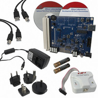
KIT DEV FOR C8051F996
Manufacturer
Silicon Laboratories Inc
Type
MCUr
Datasheets
1.C8051F996DK.pdf
(24 pages)
2.C8051F996DK.pdf
(2 pages)
3.C8051F996DK.pdf
(4 pages)
4.C8051F996DK.pdf
(322 pages)
Specifications of C8051F996DK
Contents
Board, Batteries, Cables, CDs, Debug Adapter, Documentation, Power Adapter
Processor To Be Evaluated
C8051F996
Processor Series
C8051F98x
Interface Type
USB
Operating Supply Voltage
3 V
Lead Free Status / RoHS Status
Lead free / RoHS Compliant
For Use With/related Products
C8051F996
Lead Free Status / Rohs Status
Lead free / RoHS Compliant
Other names
336-1963


SFR Definition 5.2. ADC0CF: ADC0 Configuration
SFR Page = 0x0; SFR Address = 0x97
Name
Reset
Bit
Type
7:3
2
1
0
Bit
AD0SC[4:0] ADC0 SAR Conversion Clock Divider.
AMP0GN
AD08BE
AD0TM
Name
7
1
SAR Conversion clock is derived from FCLK by the following equation, where
AD0SC refers to the 5-bit value held in bits AD0SC[4:0]. SAR Conversion clock
requirements are given in Table 4.10.
BURSTEN = 0: FCLK is the current system clock.
BURSTEN = 1: FCLK is the 20 MHz low power oscillator, independent of the system
clock.
ADC0 8-Bit Mode Enable.
0: ADC0 operates in 10-bit mode (normal operation).
1: ADC0 operates in 8-bit mode.
ADC0 Track Mode.
Selects between Normal or Delayed Tracking Modes.
0: Normal Track Mode: When ADC0 is enabled, conversion begins immediately fol-
lowing the start-of-conversion signal.
1: Delayed Track Mode: When ADC0 is enabled, conversion begins 3 SAR clock
cycles following the start-of-conversion signal. The ADC is allowed to track during
this time.
ADC0 Gain Control.
0: The on-chip PGA gain is 0.5.
1: The on-chip PGA gain is 1.
*Round the result up.
AD0SC
CLK
6
1
SAR
=
=
AD0SC[4:0]
------------------- - 1
CLK
or
FCLK
----------------------------
AD0SC
R/W
5
1
FCLK
SAR
–
+
1
*
Rev. 1.0
4
1
C8051F99x-C8051F98x
Function
3
1
AD08BE
R/W
2
0
AD0TM
R/W
1
0
AMP0GN
R/W
0
0
73
Related parts for C8051F996DK
Image
Part Number
Description
Manufacturer
Datasheet
Request
R

Part Number:
Description:
SMD/C°/SINGLE-ENDED OUTPUT SILICON OSCILLATOR
Manufacturer:
Silicon Laboratories Inc
Part Number:
Description:
Manufacturer:
Silicon Laboratories Inc
Datasheet:
Part Number:
Description:
N/A N/A/SI4010 AES KEYFOB DEMO WITH LCD RX
Manufacturer:
Silicon Laboratories Inc
Datasheet:
Part Number:
Description:
N/A N/A/SI4010 SIMPLIFIED KEY FOB DEMO WITH LED RX
Manufacturer:
Silicon Laboratories Inc
Datasheet:
Part Number:
Description:
N/A/-40 TO 85 OC/EZLINK MODULE; F930/4432 HIGH BAND (REV E/B1)
Manufacturer:
Silicon Laboratories Inc
Part Number:
Description:
EZLink Module; F930/4432 Low Band (rev e/B1)
Manufacturer:
Silicon Laboratories Inc
Part Number:
Description:
I°/4460 10 DBM RADIO TEST CARD 434 MHZ
Manufacturer:
Silicon Laboratories Inc
Part Number:
Description:
I°/4461 14 DBM RADIO TEST CARD 868 MHZ
Manufacturer:
Silicon Laboratories Inc
Part Number:
Description:
I°/4463 20 DBM RFSWITCH RADIO TEST CARD 460 MHZ
Manufacturer:
Silicon Laboratories Inc
Part Number:
Description:
I°/4463 20 DBM RADIO TEST CARD 868 MHZ
Manufacturer:
Silicon Laboratories Inc
Part Number:
Description:
I°/4463 27 DBM RADIO TEST CARD 868 MHZ
Manufacturer:
Silicon Laboratories Inc
Part Number:
Description:
I°/4463 SKYWORKS 30 DBM RADIO TEST CARD 915 MHZ
Manufacturer:
Silicon Laboratories Inc
Part Number:
Description:
N/A N/A/-40 TO 85 OC/4463 RFMD 30 DBM RADIO TEST CARD 915 MHZ
Manufacturer:
Silicon Laboratories Inc
Part Number:
Description:
I°/4463 20 DBM RADIO TEST CARD 169 MHZ
Manufacturer:
Silicon Laboratories Inc