C8051F996DK Silicon Laboratories Inc, C8051F996DK Datasheet - Page 55
C8051F996DK
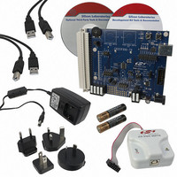
Manufacturer Part Number
C8051F996DK
Description
KIT DEV FOR C8051F996
Manufacturer
Silicon Laboratories Inc
Type
MCUr
Datasheets
1.C8051F996DK.pdf
(24 pages)
2.C8051F996DK.pdf
(2 pages)
3.C8051F996DK.pdf
(4 pages)
4.C8051F996DK.pdf
(322 pages)
Specifications of C8051F996DK
Contents
Board, Batteries, Cables, CDs, Debug Adapter, Documentation, Power Adapter
Processor To Be Evaluated
C8051F996
Processor Series
C8051F98x
Interface Type
USB
Operating Supply Voltage
3 V
Lead Free Status / RoHS Status
Lead free / RoHS Compliant
For Use With/related Products
C8051F996
Lead Free Status / Rohs Status
Lead free / RoHS Compliant
Other names
336-1963


Table 4.4. Reset Electrical Characteristics
V
RST Output Low Voltage
RST Input High Voltage
RST Input Low Voltage
RST Input Pullup Current
VDD Monitor Threshold
(V
VDD Ramp Time for Power
On
POR Monitor Threshold
(V
Missing Clock Detector
Timeout
Minimum System Clock w/
Missing Clock Detector
Enabled
Reset Time Delay
Minimum RST Low Time to
Generate a System Reset
V
V
Current
DD
DD
DD
RST
POR
= 1.8 to 3.6 V, –40 to +85 °C unless otherwise specified.
Monitor Turn-on Time
Monitor Supply
)
)
Parameter
Time from last system clock rising edge
Recovery from Brownout (VDD Rising)
System clock frequency which triggers
Delay between release of any reset
Brownout Condition (VDD Falling)
a missing clock detector timeout
(all power modes except Sleep)
execution at location 0x0000
RST = 0.0 V, VDD = 1.8 V
RST = 0.0 V, VDD = 3.6 V
VBAT Ramp from 0–1.8 V
V
V
V
V
source and code
to reset initiation
DD
DD
DD
DD
Early Warning
Reset Trigger
I
OL
Conditions
= 2.0 to 3.6 V
= 0.9 to 2.0 V
= 2.0 to 3.6 V
= 0.9 to 2.0 V
= 1.4 mA,
Rev. 1.0
C8051F99x-C8051F98x
V
0.7 x V
DD
0.45
Min
100
1.8
1.7
15
—
—
—
—
—
—
—
—
—
—
—
– 0.6
DD
1.85
1.75
1.75
Typ
650
300
0.7
—
—
—
—
—
20
—
10
—
4
7
7
0.3 x V
1000
Max
0.6
0.6
1.9
1.8
1.0
30
10
—
—
—
—
—
—
—
—
3
DD
Units
kHz
µA
ms
µA
µs
µs
µs
ns
V
V
V
V
V
V
V
55
Related parts for C8051F996DK
Image
Part Number
Description
Manufacturer
Datasheet
Request
R

Part Number:
Description:
SMD/C°/SINGLE-ENDED OUTPUT SILICON OSCILLATOR
Manufacturer:
Silicon Laboratories Inc
Part Number:
Description:
Manufacturer:
Silicon Laboratories Inc
Datasheet:
Part Number:
Description:
N/A N/A/SI4010 AES KEYFOB DEMO WITH LCD RX
Manufacturer:
Silicon Laboratories Inc
Datasheet:
Part Number:
Description:
N/A N/A/SI4010 SIMPLIFIED KEY FOB DEMO WITH LED RX
Manufacturer:
Silicon Laboratories Inc
Datasheet:
Part Number:
Description:
N/A/-40 TO 85 OC/EZLINK MODULE; F930/4432 HIGH BAND (REV E/B1)
Manufacturer:
Silicon Laboratories Inc
Part Number:
Description:
EZLink Module; F930/4432 Low Band (rev e/B1)
Manufacturer:
Silicon Laboratories Inc
Part Number:
Description:
I°/4460 10 DBM RADIO TEST CARD 434 MHZ
Manufacturer:
Silicon Laboratories Inc
Part Number:
Description:
I°/4461 14 DBM RADIO TEST CARD 868 MHZ
Manufacturer:
Silicon Laboratories Inc
Part Number:
Description:
I°/4463 20 DBM RFSWITCH RADIO TEST CARD 460 MHZ
Manufacturer:
Silicon Laboratories Inc
Part Number:
Description:
I°/4463 20 DBM RADIO TEST CARD 868 MHZ
Manufacturer:
Silicon Laboratories Inc
Part Number:
Description:
I°/4463 27 DBM RADIO TEST CARD 868 MHZ
Manufacturer:
Silicon Laboratories Inc
Part Number:
Description:
I°/4463 SKYWORKS 30 DBM RADIO TEST CARD 915 MHZ
Manufacturer:
Silicon Laboratories Inc
Part Number:
Description:
N/A N/A/-40 TO 85 OC/4463 RFMD 30 DBM RADIO TEST CARD 915 MHZ
Manufacturer:
Silicon Laboratories Inc
Part Number:
Description:
I°/4463 20 DBM RADIO TEST CARD 169 MHZ
Manufacturer:
Silicon Laboratories Inc