C8051F996DK Silicon Laboratories Inc, C8051F996DK Datasheet - Page 92
C8051F996DK
Manufacturer Part Number
C8051F996DK
Description
KIT DEV FOR C8051F996
Manufacturer
Silicon Laboratories Inc
Type
MCUr
Datasheets
1.C8051F996DK.pdf
(24 pages)
2.C8051F996DK.pdf
(2 pages)
3.C8051F996DK.pdf
(4 pages)
4.C8051F996DK.pdf
(322 pages)
Specifications of C8051F996DK
Contents
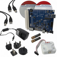
Board, Batteries, Cables, CDs, Debug Adapter, Documentation, Power Adapter
Processor To Be Evaluated
C8051F996
Processor Series
C8051F98x
Interface Type
USB
Operating Supply Voltage
3 V
Lead Free Status / RoHS Status
Lead free / RoHS Compliant
For Use With/related Products
C8051F996
Lead Free Status / Rohs Status
Lead free / RoHS Compliant
Other names
336-1963


C8051F99x-C8051F98x
7.2.
When a comparator is enabled, its output is a logic 1 if the voltage at the positive input is higher than the
voltage at the negative input. When disabled, the comparator output is a logic 0. The comparator output is
synchronized with the system clock as shown in Figure 7.2. The synchronous “latched” output (CP0) can
be polled in software (CP0OUT bit), used as an interrupt source, or routed to a Port pin (configured for
digital I/O) through the Crossbar.
The asynchronous “raw” comparator output (CP0A) is used by the low power mode wake-up logic and
reset decision logic. See the Power Options chapter and the Reset Sources chapter for more details on
how the asynchronous comparator outputs are used to make wake-up and reset decisions. The
asynchronous comparator output can also be routed directly to a Port pin through the Crossbar, and is
available for use outside the device even if the system clock is stopped.
When using a Comparator as an interrupt source, Comparator interrupts can be generated on rising-edge
and/or falling-edge comparator output transitions. Two independent interrupt flags (CP0RIF and CP0FIF)
allow software to determine which edge caused the Comparator interrupt. The comparator rising-edge and
falling-edge interrupt flags are set by hardware when a corresponding edge is detected regardless of the
interrupt enable state. Once set, these bits remain set until cleared by software.
The rising-edge and falling-edge interrupts can be individually enabled using the CP0RIE and CP0FIE
interrupt enable bits in the CPT0MD register. In order for the CP0RIF and/or CP0FIF interrupt flags to
generate an interrupt request to the CPU, the Comparator must be enabled as an interrupt source and
global interrupts must be enabled. See the Interrupt Handler chapter for additional information.
7.3.
Comparator response time may be configured in software via the CPT0MD register described on
“CPT0MD: Comparator 0 Mode Selection” on page 95. Four response time settings are available: Mode 0
(Fastest Response Time), Mode 1, Mode 2, and Mode 3 (Lowest Power). Selecting a longer response time
reduces the Comparator active supply current. The Comparator also has a low power shutdown state,
which is entered any time the comparator is disabled. Comparator rising edge and falling edge response
times are typically not equal. See Table 4.14 on page 61 for complete comparator timing and supply
current specifications.
7.4.
The Comparator features software-programmable hysteresis that can be used to stabilize the comparator
output while a transition is occurring on the input. Using the CPT0CN register, the user can program both
the amount of hysteresis voltage (referred to the input voltage) and the positive and negative-going
symmetry of this hysteresis around the threshold voltage (i.e., the comparator negative input).
Figure 7.2 shows that when positive hysteresis is enabled, the comparator output does not transition from
logic 0 to logic 1 until the comparator positive input voltage has exceeded the threshold voltage by an
amount equal to the programmed hysteresis. It also shows that when negative hysteresis is enabled, the
comparator output does not transition from logic 1 to logic 0 until the comparator positive input voltage has
fallen below the threshold voltage by an amount equal to the programmed hysteresis.
The amount of positive hysteresis is determined by the settings of the CP0HYP bits in the CPT0CN
register and the amount of negative hysteresis voltage is determined by the settings of the CP0HYN bits in
the same register. Settings of 20, 10, 5, or 0 mV can be programmed for both positive and negative
hysteresis. See Section “Table 4.14. Comparator Electrical Characteristics” on page 61 for complete
comparator hysteresis specifications.
92
Comparator Outputs
Comparator Response Time
Comparator Hysteresis
Rev. 1.0
Related parts for C8051F996DK
Image
Part Number
Description
Manufacturer
Datasheet
Request
R

Part Number:
Description:
SMD/C°/SINGLE-ENDED OUTPUT SILICON OSCILLATOR
Manufacturer:
Silicon Laboratories Inc
Part Number:
Description:
Manufacturer:
Silicon Laboratories Inc
Datasheet:
Part Number:
Description:
N/A N/A/SI4010 AES KEYFOB DEMO WITH LCD RX
Manufacturer:
Silicon Laboratories Inc
Datasheet:
Part Number:
Description:
N/A N/A/SI4010 SIMPLIFIED KEY FOB DEMO WITH LED RX
Manufacturer:
Silicon Laboratories Inc
Datasheet:
Part Number:
Description:
N/A/-40 TO 85 OC/EZLINK MODULE; F930/4432 HIGH BAND (REV E/B1)
Manufacturer:
Silicon Laboratories Inc
Part Number:
Description:
EZLink Module; F930/4432 Low Band (rev e/B1)
Manufacturer:
Silicon Laboratories Inc
Part Number:
Description:
I°/4460 10 DBM RADIO TEST CARD 434 MHZ
Manufacturer:
Silicon Laboratories Inc
Part Number:
Description:
I°/4461 14 DBM RADIO TEST CARD 868 MHZ
Manufacturer:
Silicon Laboratories Inc
Part Number:
Description:
I°/4463 20 DBM RFSWITCH RADIO TEST CARD 460 MHZ
Manufacturer:
Silicon Laboratories Inc
Part Number:
Description:
I°/4463 20 DBM RADIO TEST CARD 868 MHZ
Manufacturer:
Silicon Laboratories Inc
Part Number:
Description:
I°/4463 27 DBM RADIO TEST CARD 868 MHZ
Manufacturer:
Silicon Laboratories Inc
Part Number:
Description:
I°/4463 SKYWORKS 30 DBM RADIO TEST CARD 915 MHZ
Manufacturer:
Silicon Laboratories Inc
Part Number:
Description:
N/A N/A/-40 TO 85 OC/4463 RFMD 30 DBM RADIO TEST CARD 915 MHZ
Manufacturer:
Silicon Laboratories Inc
Part Number:
Description:
I°/4463 20 DBM RADIO TEST CARD 169 MHZ
Manufacturer:
Silicon Laboratories Inc