EVAL-ADUC832QSZ Analog Devices Inc, EVAL-ADUC832QSZ Datasheet
EVAL-ADUC832QSZ
Specifications of EVAL-ADUC832QSZ
EVAL-ADUC832QS


Related parts for EVAL-ADUC832QSZ


EVAL-ADUC832QSZ Summary of contents
Page 1
FEATURES ANALOG I/O 8-channel, 247 kSPS, 12-Bit ADC DC performance: ±1 LSB INL AC performance SNR DMA controller for high speed ADC-to-RAM capture 2 12-bit (monotonic) voltage output DACs Dual output PWM/Σ-Δ DACs On-chip temperature sensor function: ±3°C ...
Page 2
ADuC832 TABLE OF CONTENTS Features .............................................................................................. 1 Applications ....................................................................................... 1 Functional Block Diagram .............................................................. 1 General Description ......................................................................... 1 Revision History ............................................................................... 4 Specifications ..................................................................................... 6 Timing Specifications ................................................................ 10 Absolute Maximum Ratings .......................................................... 20 ESD Caution ................................................................................ 20 Pin ...
Page 3
Dual Data Pointers .......................................................................... 62 DPCON (Data Pointer Control SFR) ....................................... 62 Power Supply Monitor .................................................................... 63 PSMCON (Power Supply Monitor Control Register ) ........... 63 Watchdog Timer .............................................................................. 64 Time Interval Counter (TIC) ......................................................... 65 TIMECON (TIC Control Register) ...
Page 4
ADuC832 REVISION HISTORY 9/09—Rev Rev. A Changes to Figure 1 .......................................................................... 1 Changed 16.77 MHz to 16.78 MHz Throughout ......................... 1 Changes to Reference Input/Output, Output Voltage Parameter, Endnote 19, and Endnote 20, Table 1 ............................................ 9 Moved ...
Page 5
On-chip factory firmware supports in-circuit serial download and debug modes (via UART) as well as single-pin emulation mode via the EA pin. The ADuC832 is supported by QuickStart™ and QuickStart Plus development systems featuring low cost software and hardware development ...
Page 6
ADuC832 SPECIFICATIONS unless otherwise noted. Table 1. 1 Parameter ADC CHANNEL SPECIFICATIONS Accuracy Resolution Integral Nonlinearity Differential Nonlinearity ...
Page 7
Parameter DAC CHANNEL SPECIFICATIONS , INTERNAL BUFFER DISABLED 10 DC Accuracy Resolution Relative Accuracy 11 Differential Nonlinearity Offset Error Gain Error 4 Gain Error Mismatch Analog outputs Voltage Range 0 REFERENCE INPUT/OUTPUT Reference Output 14 Output ...
Page 8
ADuC832 1 Parameter 4 SCLOCK and RESET ONLY (Schmitt-Triggered Inputs T− V − T− CRYSTAL OSCILLATOR Logic Inputs, XTAL1 Only V , Input Low Voltage INL V , Input High Voltage INH XTAL1 Input Capacitance ...
Page 9
Parameter Power Supply Currents Power-Down Mode 4 DV Current DD AV Current DD DV Current DD Typical Additional Power Supply Currents PSM Peripheral ADC DAC 1 Temperature range: −40°C to +125°C. 2 ADC linearity is guaranteed during normal MicroConverter ...
Page 10
ADuC832 TIMING SPECIFICATIONS Table 2. Clock Input (External Clock Applied on XTAL1 Parameter Description t XTAL1 period (see Figure ...
Page 11
Table 3. External Program Memory Read Cycle Parameter 1 Description t ALE pulse width LHLL t Address valid to ALE low AVLL t Address hold after ALE low LLAX t ALE low to valid instruction in LLIV t ALE low ...
Page 12
ADuC832 Table 4. External Data Memory Read Cycle Parameter 1 Description t RD pulse width RLRH t Address valid before ALE low AVLL t Address hold after ALE low LLAX t RD low to valid data in RLDV t Data ...
Page 13
Table 5. External Data Memory Write Cycle Parameter 1 Description t WR pulse width WLWH t Address valid before ALE low AVLL t Address hold after ALE low LLAX t ALE low to WR low LLWL t Address valid to ...
Page 14
ADuC832 Table 6. UART Timing (Shift Register Mode) Parameter 1 Description t Serial port clock cycle time XLXL t Output data setup to clock QVXH t Input data setup to clock DVXH t Input data hold after clock XHDX t ...
Page 15
Table 7. I C-Compatible Interface Timing 1 Parameter Description t SCLOCK low pulse width L t SCLOCK high pulse width H t Start condition hold time SHD t Data setup time DSU t Data hold time DHD t Setup ...
Page 16
ADuC832 Table 8. SPI Master Mode Timing (CPHA = 1) 1 Parameter Description t SCLOCK low pulse width SL t SCLOCK high pulse width SH t Data output valid after SCLOCK edge DAV t Data input setup time before SCLOCK ...
Page 17
Table 9. SPI Master Mode Timing (CPHA = 0) 1 Parameter Description t SCLOCK low pulse width SL t SCLOCK high pulse width SH t Data output valid after SCLOCK edge DAV t Data output setup before SCLOCK edge DOSU ...
Page 18
ADuC832 Table 10. SPI Slave Mode Timing (CPHA = 1) 1 Parameter Description SCLOCK edge SS t SCLOCK low pulse width SL t SCLOCK high pulse width SH t Data output valid after SCLOCK edge DAV t ...
Page 19
Table 11. SPI Slave Mode Timing (CPHA = 0) 1 Parameter Description SCLOCK edge SS t SCLOCK low pulse width SL t SCLOCK high pulse width SH t Data output valid after SCLOCK edge DAV t Data ...
Page 20
ADuC832 ABSOLUTE MAXIMUM RATINGS T = 25°C, unless otherwise noted. A Table 12. Parameter AGND to DGND DV to DGND AGND DD DD Digital Input Voltage to DGND Digital Output Voltage to DGND ...
Page 21
PIN CONFIGURATIONS AND FUNCTION DESCRIPTIONS P1.0/ADC0/T2 1 PIN 1 P1.1/ADC1/T2EX IDENTIFIER 2 P1.2/ADC2 3 P1.3/ADC3 AGND 6 ADuC832 C 7 TOP VIEW REF ...
Page 22
ADuC832 Pin No. Mnemonic MQFP V 8 REF DAC0 9 DAC1 10 P1.4/ADC4 11 P1.5/ADC5/SS 12 P1.6/ADC6 13 P1.7/ADC7 14 RESET 15 P3.0/RxD 16 P3.1/TxD 17 18 P3.2/INT0 19 P3.3/INT1/MISO/PWM1 DV 20, 34 DGND 21, 35, 47 LFCSP ...
Page 23
Pin No. Mnemonic MQFP P3.4/T0/PWMC/PWM0/EXTCLK 22 P3.5/T1/CONVST 23 P3.6/ P3.7/RD SCLOCK 26 SDATA/MOSI 27 P2.0/A8/A16 28 P2.1/A9/A17 29 P2.2/A10/A18 30 P2.3/A11/A19 31 XTAL1 32 LFCSP Type Description 24 I/O Input/Output Port 3 (P3.4). Port bidirectional ...
Page 24
ADuC832 Pin No. Mnemonic MQFP XTAL2 33 P2.4/A12/A20 36 P2.5/A13/A21 37 P2.6/PWM0/A14/A22 38 P2.7/PWM1/A15/A23 PSEN 41 ALE 42 P0.0/AD0 43 P0.1/AD1 44 LFCSP Type Description 35 O Output of the Inverting Oscillator Amplifier. 39 I/O Input/Output Port ...
Page 25
Pin No. Mnemonic MQFP P0.2/AD2 45 P0.3/AD3 46 P0.4/AD4 49 P0.5/AD5 50 P0.6/AD6 51 P0.7/AD7 52 LFCSP Type Description 48 I/O Input/Output Port 0 (P0.2). Port 8-Bit Open-Drain Bidirectional I/O Port. Port 0 pins that have 1s ...
Page 26
ADuC832 TYPICAL PERFORMANCE CHARACTERISTICS 1.0 0.8 0.6 0.4 0.2 0 –0.2 –0.4 –0.6 –0.8 –1.0 0 511 1023 1535 2047 2559 ADC CODES Figure 16. Typical INL Error, V 1.0 0.8 0.6 0.4 0.2 0 –0.2 –0.4 –0.6 –0.8 –1.0 ...
Page 27
AV f 0.4 0.2 0 –0.2 –0.4 –0.6 0.5 1.0 1.5 2.0 2.5 EXTERNAL REFERENCE (V) Figure 22. Typical Worst-Case DNL Error vs 0.5 0.3 0.1 –0.1 –0.3 –0.5 –0.7 0.5 1.0 1.5 2.0 ...
Page 28
ADuC832 0.5 1.0 1.5 2.0 EXTERNAL REFERENCE (V) Figure 28. Typical Dynamic Performance vs 0.5 1.0 1.5 2.0 EXTERNAL REFERENCE (V) Figure 29. Typical Dynamic ...
Page 29
TERMINOLOGY ADC SPECIFICATIONS Integral Nonlinearity This is the maximum deviation of any code from a straight line passing through the endpoints of the ADC transfer function. The endpoints of the transfer function are zero scale, a point ½ LSB below ...
Page 30
ADuC832 EXPLANATION OF TYPICAL PERFORMANCE PLOTS The plots presented in the Typical Performance Characteristics section illustrate typical performance of the ADuC832 under various operating conditions. Figure 16 and Figure 17 show typical ADC integral nonlinearity (INL) errors from ADC Code ...
Page 31
MEMORY ORGANIZATION The ADuC832 contains four different memory blocks: • on-chip Flash/EE program memory • on-chip Flash/EE data memory • 256 bytes of general-purpose RAM • internal XRAM FLASH/EE PROGRAM MEMORY ...
Page 32
ADuC832 EXTERNAL DATA MEMORY (EXTERNAL XRAM) Similar to a standard 8051-compatible core, the ADuC832 can access external data memory using a MOVX instruction. The MOVX instruction automatically outputs the various control strobes required to access the data memory. The ADuC832, ...
Page 33
SPECIAL FUNCTION REGISTERS (SFRS) The SFR space is mapped into the upper 128 bytes of internal data memory space and accessed by direct addressing only. It provides an interface between the CPU and all on-chip peripher- als. A block diagram ...
Page 34
ADuC832 SPECIAL FUNCTION REGISTERS All registers except the program counter and the four general- purpose register banks reside in the special function register (SFR) area. The SFR registers include control, configuration, and data registers that provide an interface between the ...
Page 35
ADC CIRCUIT INFORMATION GENERAL OVERVIEW The ADC conversion block incorporates a fast, 8-channel, 12-bit, single-supply ADC. This block provides the user with multichannel mux, track/hold, on-chip reference, calibration features, and an ADC. All components in this block are easily configured ...
Page 36
ADuC832 ADCCON1 (ADC Control SFR 1) SFR Address: EFH SFR Power-On Default Value: 00H Bit Addressable: No Table 16. ADCCON1 SFR Bit Designations Bit Name Description [7] MD1 The mode bit selects the active operating mode of the ADC. Set ...
Page 37
ADCCON2 (ADC Control SFR 2) SFR Address: D8H SFR Power-On Default Value: 00H Bit Addressable: Yes Table 17. ADCCON2 SFR Bit Designations Bit Name Description [7] ADCI The ADC interrupt bit (ADCI) is set by hardware at the end of ...
Page 38
ADuC832 ADCCON3 (ADC Control SFR 3) SFR Address: F5H SFR Power-On Default Value: 00H Bit Addressable: No Table 18. ADCCON3 SFR Bit Designations Bit Name Description [7] Busy The ADC busy status bit is a read-only status bit that is ...
Page 39
DRIVING THE ANALOG-TO-DIGITAL CONVERTER The ADC incorporates a successive approximation (SAR) architec- ture involving a charge-sampled input stage. Figure 39 shows the equivalent circuit of the analog input section. Each ADC conversion is divided into two distinct phases as defined ...
Page 40
ADuC832 Table 20. Some Single-Supply Op Amps Op Amp Model Characteristics OP281/OP481 Micropower OP191/OP291/OP491 I/O Good OP196/OP296/OP496 I micropower, low cost DD OP183/OP249 High gain-bandwidth product (GBP) OP162/OP262/OP462 High GBP, micro package AD820/AD822/AD824 FET ...
Page 41
ADuC832 51Ω BAND GAP V DD REFERENCE EXTERNAL VOLTAGE REFERENCE BUFFER V REF 8 0.1µF C REF 7 0.1µF Figure 43. Using an External Voltage Reference CONFIGURING THE ADC The ADuC832’s successive approximation ADC is driven by a divided down ...
Page 42
ADuC832 When the DMA conversions are completed, the ADC interrupt bit, ADCI, is set by hardware and the external SRAM contains the new ADC conversion results as shown in Figure 45. Note that no result is written to the last ...
Page 43
CALIBRATING THE ADC There are two hardware calibration modes provided that can be easily initiated by user software. The ADCCON3 SFR is used to calibrate the ADC. The typical bit (ADCCON3[1]) and the CS3 to CS0 bits (ADCCON2[3:0]) set up ...
Page 44
ADuC832 INITIATING CALIBRATION IN CODE When calibrating the ADC using ADCCON1, the ADC should be set up into the configuration in which it will be used. The ADCCON3 register can then be used to set up the device and calibrate ...
Page 45
NONVOLATILE FLASH/EE MEMORY FLASH/EE MEMORY OVERVIEW The ADuC832 incorporates Flash/EE memory technology on chip to provide the user with nonvolatile, in-circuit, reprogramma- ble code and data memory space. Flash/EE memory is a relatively recent type of nonvolatile memory technology and ...
Page 46
ADuC832 300 250 200 ADI SPECIFICATION 100 YEARS MIN 55°C J 150 100 JUNCTION TEMPERATURE (°C) J Figure 48. Flash/EE Memory Data Retention USING THE FLASH/EE PROGRAM MEMORY The ...
Page 47
FLASH/EE PROGRAM MEMORY SECURITY The ADuC832 facilitates three modes of Flash/EE program memory security. These modes can be independently activated, restricting access to the internal code space. These security modes can be enabled as part of serial download protocol as ...
Page 48
ADuC832 USING THE FLASH/EE DATA MEMORY The Flash/EE data memory is configured as 1024 pages, each of four bytes. As with the other ADuC832 peripherals, the interface to this memory space is via a group of registers ...
Page 49
EXAMPLE: PROGRAMMING THE FLASH/EE DATA MEMORY To program F3H into the second byte on Page 03H of the Flash/EE data memory space while preserving the other three bytes already in this page, a typical program of the Flash/EE data array ...
Page 50
ADuC832 ADUC832 CONFIGURATION SFR (CFG832) The CFG832 SFR contains the necessary bits to configure the internal XRAM, external clock select, PWM output selection, DAC buffer, and the extended SP. By default, it configures the user into 8051 mode; that is, ...
Page 51
USER INTERFACE TO OTHER ON-CHIP ADUC832 PERIPHERALS The following section gives a brief overview of the various peripherals also available on-chip. A summary of the SFRs used to control and configure these peripherals is also given. DAC The ADuC832 incorporates ...
Page 52
ADuC832 USING THE DAC The on-chip DAC architecture consists of a resistor string DAC followed by an output buffer amplifier, the functional equivalent of which is illustrated in Figure 51. Details of the actual DAC architecture can be found in ...
Page 53
DAC LOADED WITH 0FFFH 3 1 DAC LOADED WITH 0000H SOURCE/SINK CURRENT (mA) Figure 54. Source and Sink Current Capability with V To reduce the effects of the saturation of the output amplifier at values close ...
Page 54
ADuC832 ON-CHIP PLL The ADuC832 is intended for use with a 32.768 kHz watch crystal. A PLL locks onto a multiple (512) of this to provide a stable 16.78 MHz clock for the system. The core can operate at this ...
Page 55
PULSE-WIDTH MODULATOR (PWM) The PWM on the ADuC832 is a highly flexible PWM offering programmable resolution and an input clock, and can be confi- gured for any one of six different modes of operation. Two of these modes allow the ...
Page 56
ADuC832 PWM MODES OF OPERATION MODE 0: PWM DISABLED The PWM is disabled, allowing P2.6 and P2 used as normal. MODE 1: SINGLE VARIABLE RESOLUTION PWM In Mode 1, both the pulse length and the cycle time (period) ...
Page 57
MODE 4: DUAL NRZ 16-BIT Σ-Δ DAC Mode 4 provides a high speed PWM output similar to that of a Σ-Δ DAC. Typically, this mode is used with the PWM clock equal to 16.777216 MHz. In this mode, P2.6 and ...
Page 58
ADuC832 SERIAL PERIPHERAL INTERFACE The ADuC832 integrates a complete hardware serial peripheral interface (SPI) on chip. SPI is an industry standard synchronous serial interface that allows eight bits of data to be synchronously transmitted and received simultaneously, that is, full ...
Page 59
SPIDAT (SPI Data Register) SFR Address: F7H Power-On Default Value: 00H Bit Addressable: No The SPIDAT SFR is written by the user to transmit data over the SPI interface, or read by the user read data just received by the ...
Page 60
ADuC832 2 I C-COMPATIBLE INTERFACE The ADuC832 supports a fully licensed interface is implemented as a full hardware slave and soft- ware master. SDATA is the data I/O pin and SCLOCK is the serial clock. These ...
Page 61
OVERVIEW The main features of the MicroConverter I • Only two bus lines are required; a serial data line (SDATA) and a serial clock line (SCLOCK). • master can communicate with multiple slave devices. Because each ...
Page 62
ADuC832 DUAL DATA POINTERS The ADuC832 incorporates two data pointers. The second data pointer is a shadow data pointer and is selected via the data pointer control SFR (DPCON). DPCON also includes features such as automatic hardware postincrement and postdecrement, ...
Page 63
POWER SUPPLY MONITOR As its name suggests, the power supply monitor, once enabled, monitors the DV supply on the ADuC832. It indicates when DD any of the supply pins drop below one of four user-selectable voltage trip points from 2.63 ...
Page 64
ADuC832 WATCHDOG TIMER The purpose of the watchdog timer is to generate a device reset or interrupt within a reasonable amount of time if the ADuC832 enters an erroneous state, possibly due to a programming error or electrical noise. The ...
Page 65
TIME INTERVAL COUNTER (TIC) A time interval counter is provided on chip for counting longer intervals than the standard 8051-compatible timers are capable of. The TIC is capable of timeout intervals ranging from 1/128 second to 255 hours. Furthermore, this ...
Page 66
ADuC832 INTVAL (USER TIME INTERVAL SELECT REGISTER) SFR Address: A6H Power-On Default Value: 00H Bit Addressable: No Valid Value 255 decimal User code writes the required time interval to this register. When the 8-bit interval counter is equal ...
Page 67
ON-CHIP PERIPHERALS This section gives a brief overview of the various secondary peripheral circuits that are also available to the user on chip. These remaining functions are mostly 8052 compatible (with a few additional features) and are controlled via ...
Page 68
ADuC832 them drive a logic low output voltage (V sinking 1.6 mA. P2.6 and P2.7 can also be used as PWM outputs. If they are selected as the PWM outputs via the CFG832 SFR, the PWM outputs overwrite anything written ...
Page 69
SPE = ENABLE) 2 HARDWARE (SLAVE ONLY) (OFF) 50ns GLITCH SFR REJECTION FILTER BITS MCO Q3 I2CM Figure 72. SCLOCK Pin I/O Functional Equivalent SPE = 1 ...
Page 70
ADuC832 TIMERS/COUNTERS The ADuC832 has three 16-bit timer/counters: Timer 0, Timer 1, and Timer 2. The timer/counter hardware has been included on chip to relieve the processor core of the overhead inherent in implementing timer/counter functionality in software. Each timer/counter ...
Page 71
TCON (Timer/Counter 0 and Timer/Counter 1 Control Register) SFR Address: 88H Power-On Default Value: 00H Bit Addressable: Yes Table 37. TCON SFR Bit Designations Bit Name Description [7] TF1 Timer 1 overflow flag. Set by hardware on a Timer/Counter 1 ...
Page 72
ADuC832 TIMER/COUNTER 0 AND TIMER/COUNTER 1 OPERATING MODES The following sections describe the operating modes for Timer/Counter 0 and Timer/Counter 1. Unless otherwise noted, it should be assumed that these modes of operation are the same for Timer 0 as ...
Page 73
TIMER/COUNTER 2 T2CON (TIMER/COUNTER 2 CONTROL REGISTER) SFR Address: C8H Power-On Default Value: 00H Bit Addressable: Yes Table 38. T2CON SFR Bit Designations Bit Name Description [7] TF2 Timer 2 overflow flag. Set by hardware on a Timer 2 overflow. ...
Page 74
ADuC832 TIMER/COUNTER OPERATION MODES The following sections describe the operating modes for Timer/ Counter 2. The operating modes are selected by bits in the T2CON SFR as shown in Table 39. Table 39. T2CON Operating Modes RCLK (or) TCLK CAP2 ...
Page 75
UART SERIAL INTERFACE The serial port is full duplex, meaning it can transmit and receive simultaneously also receive-buffered, meaning it can commence reception of a second byte before a previously received byte has been read from the receive ...
Page 76
ADuC832 MODE 0: 8-BIT SHIFT REGISTER MODE Mode 0 is selected by clearing both the SM0 and SM1 bits in the SCON SFR. Serial data enter and exit through RxD. TxD outputs the shift clock. Eight data bits are transmitted ...
Page 77
UART SERIAL PORT BAUD RATE GENERATION Mode 0 Baud Rate Generation The baud rate in Mode 0 is fixed. Mode 0 Baud Rate = (Core_CLK Frequency/12) Mode 2 Baud Rate Generation The baud rate in Mode 2 depends on the ...
Page 78
ADuC832 OSC. FREQ. IS DIVIDED BY 2, NOT 12. CORE 2 CLK * C/ C/ PIN NOTE AVAILABILITY OF ADDITIONAL EXTERNAL INTERRUPT T2EX PIN TRANSITION DETECTOR CORE CLK IS DEFINED BY THE CD BITS IN ...
Page 79
After the values for DIV and T3FD are calculated, the actual baud rate can be calculated using the following formula: × CORE Actual Baud Rate × + DIV For example, to obtain ...
Page 80
ADuC832 INTERRUPT SYSTEM The ADuC832 provides a total of nine interrupt sources with two priority levels. The control and configuration of the inter- rupt system is carried out through three interrupt-related SFRs: • IE—interrupt enable register • IP—interrupt priority register ...
Page 81
INTERRUPT PRIORITY The interrupt enable registers are written by the user to enable individual interrupt sources, whereas the interrupt priority registers allow the user to select one of two priority levels for each interrupt. An interrupt of a high priority ...
Page 82
ADuC832 ADUC832 HARDWARE DESIGN CONSIDERATIONS This section outlines some of the key hardware design considerations that must be addressed when integrating the ADuC832 into any hardware system. CLOCK OSCILLATOR The clock source for the ADuC832 can be generated by the ...
Page 83
ADuC832 P0 LATCH ALE Figure 88. External Data Memory Interface (64 kB Address Space) If access to more than RAM is desired, a feature unique to the ADuC832 allows addressing ...
Page 84
ADuC832 POWER CONSUMPTION The currents consumed by the various sections of the ADuC832 are shown in Table 50. The core values given represent the current drawn and the rest (ADC, DAC, voltage DD reference) are pulled by ...
Page 85
GROUNDING AND BOARD LAYOUT RECOMMENDATIONS As with all high resolution data converters, special attention must be paid to grounding and PCB layout of ADuC832- based designs to achieve optimum performance from the ADC and DACs. Although the ADuC832 has separate ...
Page 86
ADuC832 ANALOG INPUT V OUTPUT REF DAC OUTPUT P1.0ADC0/ AGND ADuC832 C REF V REF DAC0 10 DAC1 ...
Page 87
OTHER HARDWARE CONSIDERATIONS To facilitate in-circuit programming, plus in-circuit debug and emulation options, implement some simple connection points in the hardware that allow easy access to download, debug, and emulation modes. IN-CIRCUIT SERIAL DOWNLOAD ACCESS Nearly all ADuC832 designs can ...
Page 88
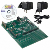
... PC-based (Windows® compatible) hardware and software development tools. Table 51. QuickStart Components Component Description Hardware ADuC832 evaluation board and serial port programming cable Software Serial download software; incorporates 8051 assembler and serial port debugger Miscellaneous CD-ROM documentation and prototype device Hardware contents include: • ...
Page 89
... ADuC832BCP-REEL −40°C to +85°C 1 ADuC832BCPZ −40°C to +85°C 1 ADuC832BCPZ-REEL −40°C to +85°C 1 ADuC832BSZ −40°C to +125°C 1 ADuC832BSZ-REEL −40°C to +125°C 1 EVAL-ADuC832QSZ RoHS Compliant Part. 2.45 1.03 MAX 0.88 0. SEATING PLANE 10° 6° 2° 0.23 VIEW A 0 ...
Page 90
ADuC832 NOTES Rev Page ...
Page 91
NOTES Rev Page ADuC832 ...
Page 92
ADuC832 NOTES 2 Purchase of licensed I C components of Analog Devices or one of its sublicensed associated companies conveys a license for the purchaser under the Philips I 2 Rights to use the ADuC832 system, ...