EVAL-ADUC832QSZ Analog Devices Inc, EVAL-ADUC832QSZ Datasheet - Page 22
EVAL-ADUC832QSZ
Manufacturer Part Number
EVAL-ADUC832QSZ
Description
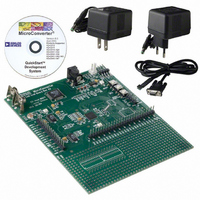
KIT DEV FOR ADUC832 QUICK START
Manufacturer
Analog Devices Inc
Series
QuickStart™ Kitr
Type
MCUr
Specifications of EVAL-ADUC832QSZ
Contents
Evaluation Board, Cable, Power Supply, Software and Documentation
Lead Free Status / RoHS Status
Lead free / RoHS Compliant
For Use With/related Products
ADuC832
Lead Free Status / RoHS Status
Compliant, Lead free / RoHS Compliant
Other names
EVAL-ADUC832QS
EVAL-ADUC832QS
EVAL-ADUC832QS


ADuC832
Mnemonic
V
DAC0
DAC1
P1.4/ADC4
P1.5/ADC5/SS
P1.6/ADC6
P1.7/ADC7
RESET
P3.0/RxD
P3.1/TxD
P3.2/INT0
P3.3/INT1/MISO/PWM1
DV
DGND
REF
DD
16
MQFP
8
9
10
11
12
13
14
15
17
18
19
20, 34,
48
21, 35,
47
Pin No.
LFCSP
10
11
12
13
14
15
16
17
18
19
20
21
22, 36,
51
23, 37,
38, 50
Type
I/O
O
O
I
I
I
I
I
I
I
I
I
I
I/O
I
I/O
O
I
I
I
I
I/O
O
P
G
Description
Reference Input/Output. This pin is connected to the internal reference through a
series resistor and is the reference source for the analog-to-digital converter. The
nominal internal reference voltage is 2.5 V, which appears at the pin. See the Voltage
Reference Connections section on how to connect an external reference.
Voltage Output from DAC0.
Voltage Output from DAC1.
Input Port 1 (P1.4). Port 1 is an 8-bit input port only. Unlike other ports, Port 1 defaults
to analog input mode. To configure any Port 1 pin as a digital input, write a 0 to the
Port 1 bit. Port 1 pins are multifunctional and share the following functionality.
Single-Ended Analog Input (ADC4). Channel selection is via ADCCON2 SFR.
Input Port 1 (P1.5). Port 1 is an 8-bit input port only. Unlike other ports, Port 1 defaults
to analog input mode. To configure any of these Port Pins as a digital input, write a 0
to the port bit. Port 1 pins are multifunction and share the following functionality.
Single-Ended Analog Input (ADC5). Channel selection is via ADCCON2 SFR.
Slave Select Input for the SPI Interface (SS).
Input Port 1 (P1.6). Port 1 is an 8-bit input port only. Unlike other ports, Port 1 defaults
to analog input mode. To configure any Port 1 pin as a digital input, write a 0 to the
Port 1 bit. Port 1 pins are multifunctional and share the following functionality.
Single-Ended Analog Input (ADC6). Channel selection is via ADCCON2 SFR.
Input Port 1 (P1.7). Port 1 is an 8-bit input port only. Unlike other ports, Port 1
defaults to Analog Input mode. To configure any Port 1 pin as a digital input,
write a 0 to the Port 1 bit. Port 1 pins are multifunctional and share the following
functionality.
Single-Ended Analog Input (ADC7). Channel selection is via ADCCON2 SFR.
running resets the device.
Input/Output Port 3 (P3.0). Port 3 is a bidirectional port with internal pull-up resistors.
Port 3 pins that have 1s written to them are pulled high by the internal pull-up
resistors, and in that state can be used as inputs. As inputs, Port 3 pins being pulled
externally low sources current because of the internal pull-up resistors.
Receiver Data Input (Asynchronous) or Data Input/Output (Synchronous) of Serial
(UART) Port (RxD).
Port 3 pins that have 1s written to them are pulled high by the internal pull-up
resistors, and in that state can be used as inputs. As inputs, Port 3 pins being pulled
externally low sources current because of the internal pull-up resistors.
Transmitter Data Output (Asynchronous) or Clock Output (Synchronous) of Serial
(UART) Port (TxD).
Port 3 pins that have 1s written to them are pulled high by the internal pull-up
resistors, and in that state can be used as inputs. As inputs, Port 3 pins being pulled
externally low sources current because of the internal pull-up resistors.
Interrupt 0 (INT0). This programmable edge or level triggered interrupt input can be
programmed to one of two priority levels. This pin can also be used as a gate control
input to Timer 0.
Port 3 pins that have 1s written to them are pulled high by the internal pull-up
resistors, and in that state can be used as inputs. As inputs, Port 3 pins being pulled
externally low sources current because of the internal pull-up resistors.
Interrupt 1 (INT1). This programmable edge or level triggered interrupt input can be
programmed to one of two priority levels. This pin can also be used as a gate control
input to Timer 1.
SPI Master Input/Slave Output Data I/O Pin for SPI Serial Interface (MISO).
PWM1 Voltage Output (PWM1). See the ADuC832 Configuration SFR (CFG832) section
for further information.
Digital Positive Supply Voltage, 3 V or 5 V Nominal.
Digital Ground. Ground reference point for the digital circuitry.
Digital Input. A high level on this pin for 24 master clock cycles while the oscillator is
Input/Output Port 3 (P3.1). Port 3 is a bidirectional port with internal pull-up resistors.
Input/Output Port 3 (P3.2). Port 3 is a bidirectional port with internal pull-up resistors.
Input/Output Port 3 (P3.3). Port 3 is a bidirectional port with internal pull-up resistors.
Rev. A | Page 22 of 92
Related parts for EVAL-ADUC832QSZ
Image
Part Number
Description
Manufacturer
Datasheet
Request
R


Part Number:
Description:
BOARD EVAL FOR SI270X-A
Manufacturer:
Silicon Laboratories Inc
Datasheet:

Part Number:
Description:
BUCK CONV REF DESIGN KIT IP1201
Manufacturer:
International Rectifier
Datasheet:
Part Number:
Description:
BOARD DEMO SYNC DUAL BUCK CNVTER
Manufacturer:
International Rectifier
Datasheet:
Part Number:
Description:
BOARD DEMO SYNC BUCK CONVETER
Manufacturer:
International Rectifier
Datasheet:

Part Number:
Description:
EVALBOARD/EB Omnidirectional microphone - Analog
Manufacturer:
Analog Devices
Datasheet:
Part Number:
Description:
EVALBOARD/EB Omnidirectional microphone - Analog
Manufacturer:
Analog Devices
Datasheet:


Part Number:
Description:
BOARD EVAL LED DRIVER LT3756
Manufacturer:
Linear Technology
Datasheet:

Part Number:
Description:
BOARD EVAL FOR AD7741/7742
Manufacturer:
Analog Devices Inc
Datasheet:

Part Number:
Description:
±1.7g Dual-Axis IMEMS Accelerometer Evaluation Board
Manufacturer:
Analog Devices Inc
Datasheet:

Part Number:
Description:
IC MULTIPLIER ANALOG 8-SOIC T/R
Manufacturer:
Analog Devices Inc
Datasheet:

Part Number:
Description:
IC ANALOG MULTIPLIER 8-DIP
Manufacturer:
Analog Devices Inc
Datasheet:
Part Number:
Description:
IC ANALOG MULTIPLIER 8-SOIC
Manufacturer:
Analog Devices Inc
Datasheet:
Part Number:
Description:
IC ANALOG MULTIPLIER 8-DIP
Manufacturer:
Analog Devices Inc
Datasheet: