EVAL-ADUC832QSZ Analog Devices Inc, EVAL-ADUC832QSZ Datasheet - Page 83
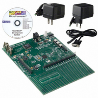
EVAL-ADUC832QSZ
Manufacturer Part Number
EVAL-ADUC832QSZ
Description
KIT DEV FOR ADUC832 QUICK START
Manufacturer
Analog Devices Inc
Series
QuickStart™ Kitr
Type
MCUr
Specifications of EVAL-ADUC832QSZ
Contents
Evaluation Board, Cable, Power Supply, Software and Documentation
Lead Free Status / RoHS Status
Lead free / RoHS Compliant
For Use With/related Products
ADuC832
Lead Free Status / RoHS Status
Compliant, Lead free / RoHS Compliant
Other names
EVAL-ADUC832QS
EVAL-ADUC832QS
EVAL-ADUC832QS


If access to more than 64 kB of RAM is desired, a feature unique
to the ADuC832 allows addressing up to 16 MB of external
RAM simply by adding an additional latch, as illustrated in
Figure 89.
In either implementation, Port 0 (P0) serves as a multiplexed
address/data bus. It emits the low byte of the data pointer (DPL)
as an address, which is latched by a pulse of ALE prior to data
being placed on the bus by the ADuC832 (write operation) or
the SRAM (read operation). Port 2 (P2) provides the data
pointer page byte (DPP) to be latched by ALE, followed by the
data pointer high byte (DPH). If no latch is connected to P2,
DPP is ignored by the SRAM, and the 8051 standard of 64 kB
external data memory access is maintained.
POWER SUPPLIES
The ADuC832 operational power supply voltage range is 2.7 V
to 5.25 V. Although the guaranteed data sheet specifications are
given only for power supplies within 2.7 V to 3.6 V or 10% of
the nominal 5 V level, the chip functions equally well at any
power supply level between 2.7 V and 5.5 V.
Note that Figure 90 and Figure 91 refer to the MQFP package.
For the LFCSP package, connect the extra DV
and AGND in the same manner.
Separate analog and digital power supply pins (AV
respectively) allow AV
often present on the system DV
and DV
they must remain within 0.3 V of one another at all times to
Figure 89. External Data Memory Interface (16 MB Address Space)
Figure 88. External Data Memory Interface (64 kB Address Space)
ADuC832
ADuC832
DD
can be powered from two separate supplies if desired,
ALE
ALE
WR
WR
RD
RD
P0
P2
P0
P2
DD
to be relatively free of noisy digital signals
LATCH
LATCH
LATCH
DD
line. However, though AV
A0 TO A7
A8 TO A15
D0 TO D7
(DATA)
A0 TO A7
A8 TO A15
A16 TO A23
OE
WE
D0 TO D7
(DATA)
OE
WE
DD
, DGND, AV
SRAM
SRAM
DD
and DV
DD
DD
Rev. A | Page 83 of 92
,
DD
,
avoid damaging the chip (as per the Absolute Maximum Ratings
section). Therefore, it is recommended that, unless AV
DV
diodes be connected between them as shown in Figure 90.
As an alternative to providing two separate power supplies,
the user can keep AV
and/or ferrite bead between it and DV
AV
shown in Figure 91. With this configuration, other analog circuitry
(such as op amps and voltage reference) can be powered from
the AV
to-back Schottky diodes between AV
from power-up and power-down transient conditions that may
separate the two supply voltages momentarily.
Note that, in both Figure 90 and Figure 91, a large value (10 μF)
reservoir capacitor is connected to DV
capacitor is connected to AV
capacitors are located at each AV
dard design practice, be sure to include all of these capacitors,
and ensure that the smaller capacitors are close to each AV
pin with trace lengths as short as possible. Connect the ground
terminal of each of these capacitors directly to the underlying
ground plane. Finally, it should also be noted that, at all times,
the analog and digital ground pins on the ADuC832 must be
referenced to the same system ground reference point.
DD
DD
separately to ground. An example of this configuration is
are connected directly together, back-to-back Schottky
DD
DIGITAL SUPPLY
supply line as well. The user should still include back-
0.1µF
0.1µF
DIGITAL SUPPLY
Figure 91. External Single-Supply Connections
Figure 90. External Dual-Supply Connections
10µF
10µF
DD
quiet by placing a small series resistor
DV
DGND
DV
DGND
DD
BEAD
DD
DD
ADuC832
. Also, local small-value (0.1 μF)
ADuC832
DD
pin of the chip. As per stan-
1.6Ω
DD
AGND
DD
AGND
AV
DD
AV
and DV
ANALOG SUPPLY
, and then decoupling
DD
DD
and a separate 10 μF
10µF
10µF
DD
0.1µF
0.1µF
ADuC832
to protect
DD
and
DD
Related parts for EVAL-ADUC832QSZ
Image
Part Number
Description
Manufacturer
Datasheet
Request
R


Part Number:
Description:
BOARD EVAL FOR SI270X-A
Manufacturer:
Silicon Laboratories Inc
Datasheet:

Part Number:
Description:
BUCK CONV REF DESIGN KIT IP1201
Manufacturer:
International Rectifier
Datasheet:
Part Number:
Description:
BOARD DEMO SYNC DUAL BUCK CNVTER
Manufacturer:
International Rectifier
Datasheet:
Part Number:
Description:
BOARD DEMO SYNC BUCK CONVETER
Manufacturer:
International Rectifier
Datasheet:

Part Number:
Description:
EVALBOARD/EB Omnidirectional microphone - Analog
Manufacturer:
Analog Devices
Datasheet:
Part Number:
Description:
EVALBOARD/EB Omnidirectional microphone - Analog
Manufacturer:
Analog Devices
Datasheet:


Part Number:
Description:
BOARD EVAL LED DRIVER LT3756
Manufacturer:
Linear Technology
Datasheet:

Part Number:
Description:
BOARD EVAL FOR AD7741/7742
Manufacturer:
Analog Devices Inc
Datasheet:

Part Number:
Description:
±1.7g Dual-Axis IMEMS Accelerometer Evaluation Board
Manufacturer:
Analog Devices Inc
Datasheet:

Part Number:
Description:
IC MULTIPLIER ANALOG 8-SOIC T/R
Manufacturer:
Analog Devices Inc
Datasheet:

Part Number:
Description:
IC ANALOG MULTIPLIER 8-DIP
Manufacturer:
Analog Devices Inc
Datasheet:
Part Number:
Description:
IC ANALOG MULTIPLIER 8-SOIC
Manufacturer:
Analog Devices Inc
Datasheet:
Part Number:
Description:
IC ANALOG MULTIPLIER 8-DIP
Manufacturer:
Analog Devices Inc
Datasheet: