EVAL-ADUC832QSZ Analog Devices Inc, EVAL-ADUC832QSZ Datasheet - Page 36
EVAL-ADUC832QSZ
Manufacturer Part Number
EVAL-ADUC832QSZ
Description
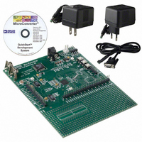
KIT DEV FOR ADUC832 QUICK START
Manufacturer
Analog Devices Inc
Series
QuickStart™ Kitr
Type
MCUr
Specifications of EVAL-ADUC832QSZ
Contents
Evaluation Board, Cable, Power Supply, Software and Documentation
Lead Free Status / RoHS Status
Lead free / RoHS Compliant
For Use With/related Products
ADuC832
Lead Free Status / RoHS Status
Compliant, Lead free / RoHS Compliant
Other names
EVAL-ADUC832QS
EVAL-ADUC832QS
EVAL-ADUC832QS


ADuC832
ADCCON1 (ADC Control SFR 1)
SFR Address:
SFR Power-On Default Value:
Bit Addressable:
Table 16. ADCCON1 SFR Bit Designations
Bit
[7]
[6]
[5]
[4]
[3:2]
[1]
[0]
Name
MD1
EXT_REF
CK1
CK0
AQ[1:0]
T2C
EXC
Description
The mode bit selects the active operating mode of the ADC. Set by the user to power up the ADC. Cleared by the user
to power down the ADC.
Set by the user to select an external reference. Cleared by the user to use the internal reference.
The ADC clock divide bits (CK1, CK0) select the divide ratio for the PLL master clock used to generate the
ADC clock. To ensure correct ADC operation, the divider ratio must be chosen to reduce the ADC clock to ≤4.5 MHz. A
typical ADC conversion requires 17 ADC clocks. The divider ratio is selected as follows:
CK1
0
0
1
1
The ADC acquisition select bits (AQ1, AQ0) select the time provided for the input track-and-hold amplifier to acquire
the input signal. An acquisition of three or more ADC clocks is recommended; clocks are selected as follows:
AQ1
0
0
1
1
The Timer 2 conversion bit (T2C) is set by the user to enable the Timer 2 overflow bit to be used as the ADC convert
start trigger input.
The external trigger enable bit (EXC) is set by the user to allow the external Pin P3.5/T1/CONVST to be used as the
active low convert start input. This input should be an active low pulse (minimum pulse width >100 ns) at the required
sample rate.
EFH
00H
No
CK0
0
1
0
1
AQ0
0
1
0
1
Rev. A | Page 36 of 92
MCLK Divider
8
4
16
32
Number of ADC Clocks
1
2
3
4
The ADCCON1 register controls conversion and acquisition
times, hardware conversion modes, and power-down modes as
detailed in Table 16.
Related parts for EVAL-ADUC832QSZ
Image
Part Number
Description
Manufacturer
Datasheet
Request
R


Part Number:
Description:
BOARD EVAL FOR SI270X-A
Manufacturer:
Silicon Laboratories Inc
Datasheet:

Part Number:
Description:
BUCK CONV REF DESIGN KIT IP1201
Manufacturer:
International Rectifier
Datasheet:
Part Number:
Description:
BOARD DEMO SYNC DUAL BUCK CNVTER
Manufacturer:
International Rectifier
Datasheet:
Part Number:
Description:
BOARD DEMO SYNC BUCK CONVETER
Manufacturer:
International Rectifier
Datasheet:

Part Number:
Description:
EVALBOARD/EB Omnidirectional microphone - Analog
Manufacturer:
Analog Devices
Datasheet:
Part Number:
Description:
EVALBOARD/EB Omnidirectional microphone - Analog
Manufacturer:
Analog Devices
Datasheet:


Part Number:
Description:
BOARD EVAL LED DRIVER LT3756
Manufacturer:
Linear Technology
Datasheet:

Part Number:
Description:
BOARD EVAL FOR AD7741/7742
Manufacturer:
Analog Devices Inc
Datasheet:

Part Number:
Description:
±1.7g Dual-Axis IMEMS Accelerometer Evaluation Board
Manufacturer:
Analog Devices Inc
Datasheet:

Part Number:
Description:
IC MULTIPLIER ANALOG 8-SOIC T/R
Manufacturer:
Analog Devices Inc
Datasheet:

Part Number:
Description:
IC ANALOG MULTIPLIER 8-DIP
Manufacturer:
Analog Devices Inc
Datasheet:
Part Number:
Description:
IC ANALOG MULTIPLIER 8-SOIC
Manufacturer:
Analog Devices Inc
Datasheet:
Part Number:
Description:
IC ANALOG MULTIPLIER 8-DIP
Manufacturer:
Analog Devices Inc
Datasheet: