EVAL-ADUC832QSZ Analog Devices Inc, EVAL-ADUC832QSZ Datasheet - Page 35
EVAL-ADUC832QSZ
Manufacturer Part Number
EVAL-ADUC832QSZ
Description
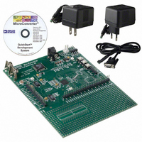
KIT DEV FOR ADUC832 QUICK START
Manufacturer
Analog Devices Inc
Series
QuickStart™ Kitr
Type
MCUr
Specifications of EVAL-ADUC832QSZ
Contents
Evaluation Board, Cable, Power Supply, Software and Documentation
Lead Free Status / RoHS Status
Lead free / RoHS Compliant
For Use With/related Products
ADuC832
Lead Free Status / RoHS Status
Compliant, Lead free / RoHS Compliant
Other names
EVAL-ADUC832QS
EVAL-ADUC832QS
EVAL-ADUC832QS


ADC CIRCUIT INFORMATION
GENERAL OVERVIEW
The ADC conversion block incorporates a fast, 8-channel,
12-bit, single-supply ADC. This block provides the user with
multichannel mux, track/hold, on-chip reference, calibration
features, and an ADC. All components in this block are easily
configured via a three-register SFR interface.
The ADC consists of a conventional successive approximation
converter based around a capacitor DAC. The converter accepts
an analog input range of 0 V to V
and factory calibrated 2.5 V reference is provided on-chip. An
external reference can be connected as described in the Voltage
Reference Connections section. This external reference can be
in the range of 1 V to AV
Single step or continuous conversion modes can be initiated in
software or alternatively by applying a convert signal to an
external pin. Timer 2 can also be configured to generate a
repetitive trigger for ADC conversions. The ADC can be
configured to operate in a DMA mode whereby the ADC block
continuously converts and captures samples to an external
RAM space without any interaction from the MCU core. This
automatic capture facility can extend through a 16 MB external
data memory space.
The ADuC832 is shipped with factory programmed calibration
coefficients that are automatically downloaded to the ADC on
power-up, ensuring optimum ADC performance. The ADC
core contains internal offset and gain calibration registers that
can be hardware calibrated to minimize system errors.
A voltage output from an on-chip band gap reference propor-
tional to absolute temperature can also be routed through the
front-end ADC multiplexer (effectively a ninth ADC channel
input) facilitating a temperature sensor implementation.
DD
.
REF
. A high precision, low drift,
Rev. A | Page 35 of 92
ADC TRANSFER FUNCTION
The analog input range for the ADC is 0 V to V
the designed code transitions occur midway between successive
integer LSB values (that is, 1/2 LSB, 3/2 LSBs, 5/2 LSBs…FS −
3/2 LSBs). The output coding is straight binary with 1 LSB =
FS/4096 or 2.5 V/4096 = 0.61 mV when V
input/output transfer characteristic for the 0 V to V
shown in Figure 37.
TYPICAL OPERATION
Once configured via the ADCCON1 to ADCCON3 SFRs, the
ADC converts the analog input and provides an ADC 12-bit
result word in the ADCDATAH/ADCDATAHL SFRs. The top
four bits of the ADCDATAH SFR are written with the channel
selection bits to identify the channel result. The format of the ADC
12-bit result word is shown in Figure 38.
TOP 4 BITS
CH–ID
111...111
111...110
111...101
111...100
000...011
000...010
000...001
000...000
OUTPUT
CODE
0V 1LSB
Figure 37. ADC Transfer Function
1LSB =
Figure 38. ADC Result Format
4096
FS
VOLTAGE INPUT
LOW 8 BITS OF THE
ADC RESULT WORD
HIGH 4 BITS OF
ADC RESULT WORD
REF
REF
= 2.5 V. The ideal
ADCDATAH SFR
ADCDATAL SFR
+FS
–1LSB
. For this range,
ADuC832
REF
range is
Related parts for EVAL-ADUC832QSZ
Image
Part Number
Description
Manufacturer
Datasheet
Request
R


Part Number:
Description:
BOARD EVAL FOR SI270X-A
Manufacturer:
Silicon Laboratories Inc
Datasheet:

Part Number:
Description:
BUCK CONV REF DESIGN KIT IP1201
Manufacturer:
International Rectifier
Datasheet:
Part Number:
Description:
BOARD DEMO SYNC DUAL BUCK CNVTER
Manufacturer:
International Rectifier
Datasheet:
Part Number:
Description:
BOARD DEMO SYNC BUCK CONVETER
Manufacturer:
International Rectifier
Datasheet:

Part Number:
Description:
EVALBOARD/EB Omnidirectional microphone - Analog
Manufacturer:
Analog Devices
Datasheet:
Part Number:
Description:
EVALBOARD/EB Omnidirectional microphone - Analog
Manufacturer:
Analog Devices
Datasheet:


Part Number:
Description:
BOARD EVAL LED DRIVER LT3756
Manufacturer:
Linear Technology
Datasheet:

Part Number:
Description:
BOARD EVAL FOR AD7741/7742
Manufacturer:
Analog Devices Inc
Datasheet:

Part Number:
Description:
±1.7g Dual-Axis IMEMS Accelerometer Evaluation Board
Manufacturer:
Analog Devices Inc
Datasheet:

Part Number:
Description:
IC MULTIPLIER ANALOG 8-SOIC T/R
Manufacturer:
Analog Devices Inc
Datasheet:

Part Number:
Description:
IC ANALOG MULTIPLIER 8-DIP
Manufacturer:
Analog Devices Inc
Datasheet:
Part Number:
Description:
IC ANALOG MULTIPLIER 8-SOIC
Manufacturer:
Analog Devices Inc
Datasheet:
Part Number:
Description:
IC ANALOG MULTIPLIER 8-DIP
Manufacturer:
Analog Devices Inc
Datasheet: