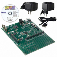
EVAL-ADUC832QSZ Analog Devices Inc, EVAL-ADUC832QSZ Datasheet - Page 57
EVAL-ADUC832QSZ
Manufacturer Part Number
EVAL-ADUC832QSZ
Description
KIT DEV FOR ADUC832 QUICK START
Manufacturer
Analog Devices Inc
Series
QuickStart™ Kitr
Type
MCUr
Specifications of EVAL-ADUC832QSZ
Contents
Evaluation Board, Cable, Power Supply, Software and Documentation
Lead Free Status / RoHS Status
Lead free / RoHS Compliant
For Use With/related Products
ADuC832
Lead Free Status / RoHS Status
Compliant, Lead free / RoHS Compliant
Other names
EVAL-ADUC832QS
EVAL-ADUC832QS
EVAL-ADUC832QS


MODE 4: DUAL NRZ 16-BIT Σ-Δ DAC
Mode 4 provides a high speed PWM output similar to that of a
Σ-Δ DAC. Typically, this mode is used with the PWM clock
equal to 16.777216 MHz.
In this mode, P2.6 and P2.7 are updated every PWM clock
PWM) PWM0 (P2.6) is high for PWM0H/PWM0L cycles and
low for (65,536 − PWM0H/L) cycles. Similarly PWM1 (P2.7) is
high for PWM1H/PWM1L cycles and low for (65,536 −
PWM1H/PWM1L) cycles.
For example, if PWM1H/L was set to 4010H (slightly above one
quarter of FS), then typically P2.7 is low for three clocks and
high for one clock (each clock is approximately 60 ns). Over
every 65,536 clocks, the PWM compensates for the fact that the
output should be slightly above one quarter of full scale by
having a high cycle followed by only two low cycles.
16.78MHz
For faster DAC outputs (at lower resolution) write 0s to the
LSBs that are not required. If, for example, only 12-bit perfor-
mance is required, then write 0s to the four LSBs. This means
that a 12-bit accurate Σ-Δ DAC output can occur at 4.096 kHz.
Similarly, writing 0s to the eight LSBs gives an 8-bit accurate
Σ-Δ DAC output at 65 kHz.
MODE 5: DUAL 8-BIT PWM
In Mode 5, the duty cycle of the PWM outputs and the resolu-
tion of the PWM outputs are individually programmable. The
maximum resolution of the PWM output is eight bits. The
output resolution is set by the PWM1L and PWM1H SFRs for
the P2.6 and P2.7 outputs, respectively. PWM0L and PWM0H
set the duty cycles of the PWM outputs at P2.6 and P2.7,
respectively. Both PWMs have same clock source and clock
divider.
(60 ns in the case of 16 MHz). Over every 65,536 cycles (16-bit
PWM0H/L = C000H
PWM1H/L = 4000H
16-BIT
16-BIT
16-BIT
16-BIT
LATCH
Figure 60. PWM Mode 4
CARRY OUT AT P1.0
CARRY OUT AT P2.7
16-BIT
16-BIT
60µs
60µs
0
0
1
0
1
0
1
1
0
0
1
0
1
0
Rev. A | Page 57 of 92
MODE 6: DUAL RZ 16-BIT Σ-Δ DAC
Mode 6 provides a high speed PWM output similar to that of a
Σ-Δ DAC. Mode 6 operates very similarly to Mode 4. However,
the key difference is that Mode 6 provides return-to-zero (RZ)
Σ-Δ DAC output. Mode 4 provides nonreturn-to-zero Σ-Δ DAC
outputs. The RZ mode ensures that any difference in the rise
and fall times does not affect the Σ-Δ DAC INL. However, the
RZ mode halves the dynamic range of the Σ-Δ DAC outputs
from 0 V − AV
mode should be used with a PWM clock divider of four.
If PWM1H is set to 4010H (slightly above one quarter of FS)
then typically P2.7 is low for three full clocks (3 × 60 ns), high
for half a clock (30 ns), and then low again for half a clock
(30 ns) before repeating itself. Over every 65,536 clocks, the
PWM compensates for the fact that the output should be slightly
above one quarter of full scale by occasionally leaving the
output high for two half clocks in four.
PWM0H/L = C000H
PWM1H/L = 4000H
16-BIT
16-BIT
16-BIT
16-BIT
4MHz
0, 3/4, 1/2, 1/4, 0
DD
down to 0 V − AV
LATCH
PWM COUNTERS
Figure 61. PWM Mode 5
Figure 62. PWM Mode 6
CARRY OUT AT P2.6
CARRY OUT AT P2.7
16-BIT
16-BIT
DD
/2. For best results, this
240 s
240 s
0 1
0
0
1
0 1
ADuC832
1
P2.6
PWM0H
0
P2.7
PWM1L
PWM1H
PWM0L
0
0
1
0
1
0
Related parts for EVAL-ADUC832QSZ
Image
Part Number
Description
Manufacturer
Datasheet
Request
R


Part Number:
Description:
BOARD EVAL FOR SI270X-A
Manufacturer:
Silicon Laboratories Inc
Datasheet:

Part Number:
Description:
BUCK CONV REF DESIGN KIT IP1201
Manufacturer:
International Rectifier
Datasheet:
Part Number:
Description:
BOARD DEMO SYNC DUAL BUCK CNVTER
Manufacturer:
International Rectifier
Datasheet:
Part Number:
Description:
BOARD DEMO SYNC BUCK CONVETER
Manufacturer:
International Rectifier
Datasheet:

Part Number:
Description:
EVALBOARD/EB Omnidirectional microphone - Analog
Manufacturer:
Analog Devices
Datasheet:
Part Number:
Description:
EVALBOARD/EB Omnidirectional microphone - Analog
Manufacturer:
Analog Devices
Datasheet:


Part Number:
Description:
BOARD EVAL LED DRIVER LT3756
Manufacturer:
Linear Technology
Datasheet:

Part Number:
Description:
BOARD EVAL FOR AD7741/7742
Manufacturer:
Analog Devices Inc
Datasheet:

Part Number:
Description:
±1.7g Dual-Axis IMEMS Accelerometer Evaluation Board
Manufacturer:
Analog Devices Inc
Datasheet:

Part Number:
Description:
IC MULTIPLIER ANALOG 8-SOIC T/R
Manufacturer:
Analog Devices Inc
Datasheet:

Part Number:
Description:
IC ANALOG MULTIPLIER 8-DIP
Manufacturer:
Analog Devices Inc
Datasheet:
Part Number:
Description:
IC ANALOG MULTIPLIER 8-SOIC
Manufacturer:
Analog Devices Inc
Datasheet:
Part Number:
Description:
IC ANALOG MULTIPLIER 8-DIP
Manufacturer:
Analog Devices Inc
Datasheet: