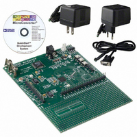
EVAL-ADUC832QSZ Analog Devices Inc, EVAL-ADUC832QSZ Datasheet - Page 10
EVAL-ADUC832QSZ
Manufacturer Part Number
EVAL-ADUC832QSZ
Description
KIT DEV FOR ADUC832 QUICK START
Manufacturer
Analog Devices Inc
Series
QuickStart™ Kitr
Type
MCUr
Specifications of EVAL-ADUC832QSZ
Contents
Evaluation Board, Cable, Power Supply, Software and Documentation
Lead Free Status / RoHS Status
Lead free / RoHS Compliant
For Use With/related Products
ADuC832
Lead Free Status / RoHS Status
Compliant, Lead free / RoHS Compliant
Other names
EVAL-ADUC832QS
EVAL-ADUC832QS
EVAL-ADUC832QS


ADuC832
TIMING SPECIFICATIONS
AV
Table 2. Clock Input (External Clock Applied on XTAL1)
Parameter
t
t
t
t
t
1/t
t
t
1
2
3
4
5
6
CK
CKL
CKH
CKR
CKF
CORE
CYC
AC inputs during testing are driven at DV
a Logic 0, as shown in Figure 4.
For timing purposes, a port pin is no longer floating when a 100 mV change from load voltage occurs. A port pin begins to float when a 100 mV change from the
loaded V
C
The ADuC832 internal PLL locks onto a multiple (512 times) the external crystal frequency of 32.768 kHz to provide a stable 16.78 MHz internal clock for the system.
The core can operate at this frequency or at a binary submultiple called Core_CLK, selected via the PLLCON SFR.
This number is measured at the default Core_CLK operating frequency of 2.09 MHz.
ADuC832 machine cycle time is nominally defined as 12/Core_CLK.
LOAD
CORE
DD
for all outputs = 80 pF, unless otherwise noted.
= 2.7 V to 3.6 V or 4.75 V to 5.25 V, DV
OH
/V
1, 2, 3
OL
level occurs, as shown in Figure 4.
DV
DD
–0.5V
0.45V
Description
XTAL1 period (see Figure 3)
XTAL1 width low (see Figure 3)
XTAL1 width high (see Figure 3)
XTAL1 rise time (see Figure 3)
XTAL1 fall time (see Figure 3)
ADuC832 core clock frequency
ADuC832 core clock period
ADuC832 machine cycle time
DD
− 0.5 V for a Logic 1 and 0.45 V for a Logic 0. Timing measurements are made at V
0.2DV
0.2DV
TEST POINTS
DD
DD
DD
= 2.7 V to 3.6 V or 4.75 V to 5.25 V; all specifications T
+ 0.9V
– 0.1V
t
CKH
Figure 4. Timing Waveform Characteristics
5
6
4
Figure 3. XTAL1 Input
Rev. A | Page 10 of 92
V
LOAD
t
CKL
V
V
LOAD
LOAD
+ 0.1V
– 0.1V
t
CKR
t
CK
0.131
0.72
Min
REFERENCE
POINTS
TIMING
32.768 kHz External Crystal
t
CKF
Typ
30.52
15.16
15.16
20
20
0.476
5.7
MIN
to T
IH
V
V
LOAD
LOAD
minimum for a Logic 1 and V
MAX
– 0.1V
+ 0.1V
, unless otherwise noted.
V
Max
16.78
91.55
LOAD
IL
maximum for
Unit
μs
μs
μs
ns
ns
MHz
μs
μs
Related parts for EVAL-ADUC832QSZ
Image
Part Number
Description
Manufacturer
Datasheet
Request
R


Part Number:
Description:
BOARD EVAL FOR SI270X-A
Manufacturer:
Silicon Laboratories Inc
Datasheet:

Part Number:
Description:
BUCK CONV REF DESIGN KIT IP1201
Manufacturer:
International Rectifier
Datasheet:
Part Number:
Description:
BOARD DEMO SYNC DUAL BUCK CNVTER
Manufacturer:
International Rectifier
Datasheet:
Part Number:
Description:
BOARD DEMO SYNC BUCK CONVETER
Manufacturer:
International Rectifier
Datasheet:

Part Number:
Description:
EVALBOARD/EB Omnidirectional microphone - Analog
Manufacturer:
Analog Devices
Datasheet:
Part Number:
Description:
EVALBOARD/EB Omnidirectional microphone - Analog
Manufacturer:
Analog Devices
Datasheet:


Part Number:
Description:
BOARD EVAL LED DRIVER LT3756
Manufacturer:
Linear Technology
Datasheet:

Part Number:
Description:
BOARD EVAL FOR AD7741/7742
Manufacturer:
Analog Devices Inc
Datasheet:

Part Number:
Description:
±1.7g Dual-Axis IMEMS Accelerometer Evaluation Board
Manufacturer:
Analog Devices Inc
Datasheet:

Part Number:
Description:
IC MULTIPLIER ANALOG 8-SOIC T/R
Manufacturer:
Analog Devices Inc
Datasheet:

Part Number:
Description:
IC ANALOG MULTIPLIER 8-DIP
Manufacturer:
Analog Devices Inc
Datasheet:
Part Number:
Description:
IC ANALOG MULTIPLIER 8-SOIC
Manufacturer:
Analog Devices Inc
Datasheet:
Part Number:
Description:
IC ANALOG MULTIPLIER 8-DIP
Manufacturer:
Analog Devices Inc
Datasheet: