TOOLSTICK540DC Silicon Laboratories Inc, TOOLSTICK540DC Datasheet - Page 131
TOOLSTICK540DC
Manufacturer Part Number
TOOLSTICK540DC
Description
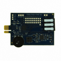
DAUGHTER CARD TOOLSTICK F540
Manufacturer
Silicon Laboratories Inc
Series
ToolStickr
Type
MCUr
Datasheets
1.TOOLSTICK540DC.pdf
(274 pages)
2.TOOLSTICK540DC.pdf
(16 pages)
3.TOOLSTICK540DC.pdf
(12 pages)
Specifications of TOOLSTICK540DC
Contents
Daughter Card
Processor To Be Evaluated
C8051F54x
Processor Series
C8051F54x
Interface Type
USB
Operating Supply Voltage
2.7 V to 3.6 V
Lead Free Status / RoHS Status
Lead free / RoHS Compliant
For Use With/related Products
C8051F54x
For Use With
336-1345 - TOOLSTICK BASE ADAPTER336-1182 - ADAPTER USB DEBUG FOR C8051FXXX
Lead Free Status / Rohs Status
Lead free / RoHS Compliant
Other names
336-1717


Important Note: If the V
is selected as a reset source. Selecting the V
lized may cause a system reset. In some applications, this reset may be undesirable. If this is not desirable
in the application, a delay should be introduced between enabling the monitor and selecting it as a reset
source. The procedure for enabling the V
state is as follows:
1. Enable the V
2. If necessary, wait for the V
3. Select the V
See Figure 16.2 for V
monitor reset. See Table 6.4 for complete electrical characteristics of the V
Note: The output of the internal voltage regulator is calibrated by the MCU immediately after any reset event. The
When programming the Flash in-system, the V
highest system reliability, the time the V
(e.g., setting the V
changing it back to the low threshold setting immediately after the Flash write operation).
Note: This delay should be omitted if software contains routines that erase or write Flash
memory.
output of the un-calibrated internal regulator could be below the high threshold setting of the VDD Monitor. If
this is the case and the V
reset (POR), the MCU will remain in reset until a POR occurs (i.e., V
POR will force the V
output of the internal regulator. The device will then exit reset and resume normal operation. It is for this reason
Silicon Labs strongly recommends that the V
value upon POR).
DD
DD
monitor as a reset source (PORSF bit in RSTSRC = 1).
DD
monitor (VDMEN bit in VDM0CN = 1).
Monitor to the high threshold setting just before the Flash write operation and then
DD
DD
DD
monitor timing; note that the power-on-reset delay is not incurred after a V
Monitor to the low threshold setting which is guaranteed to be below the un-calibrated
monitor is being turned on from a disabled state, it should be enabled before it
DD
DD
Monitor is set to the high threshold setting and if the MCU receives a non-power on
monitor to stabilize (see Table 6.4 for the V
DD
DD
Monitor is set to the high threshold setting should be minimized
monitor and configuring it as a reset source from a disabled
DD
DD
DD
Rev. 1.1
monitor as a reset source before it is enabled and stabi-
Monitor is always left in the low threshold setting (i.e., default
Monitor must be set to the high threshold setting. For the
DD
Monitor will keep the device in reset). A
DD
DD
monitor.
Monitor turn-on time).
C8051F54x
131
DD
Related parts for TOOLSTICK540DC
Image
Part Number
Description
Manufacturer
Datasheet
Request
R

Part Number:
Description:
KIT TOOL EVAL SYS IN A USB STICK
Manufacturer:
Silicon Laboratories Inc
Datasheet:

Part Number:
Description:
TOOLSTICK DEBUG ADAPTER
Manufacturer:
Silicon Laboratories Inc
Datasheet:

Part Number:
Description:
TOOLSTICK BASE ADAPTER
Manufacturer:
Silicon Laboratories Inc
Datasheet:

Part Number:
Description:
TOOLSTICK DAUGHTER CARD
Manufacturer:
Silicon Laboratories Inc
Datasheet:

Part Number:
Description:
TOOLSTICK DAUGHTER CARD
Manufacturer:
Silicon Laboratories Inc
Datasheet:

Part Number:
Description:
TOOLSTICK DAUGHTER CARD
Manufacturer:
Silicon Laboratories Inc
Datasheet:

Part Number:
Description:
TOOLSTICK PROGRAMMING ADAPTER
Manufacturer:
Silicon Laboratories Inc
Datasheet:

Part Number:
Description:
TOOLSTICK DAUGHTER CARD
Manufacturer:
Silicon Laboratories Inc
Datasheet:

Part Number:
Description:
KIT STARTER TOOLSTICK
Manufacturer:
Silicon Laboratories Inc
Datasheet:

Part Number:
Description:
KIT UNIVERSITY TOOLSTICK STARTER
Manufacturer:
Silicon Laboratories Inc
Datasheet:

Part Number:
Description:
DAUGHTER CARD TOOLSTICK F330
Manufacturer:
Silicon Laboratories Inc
Datasheet:

Part Number:
Description:
CARD DAUGHTER UNIVRSTY TOOLSTICK
Manufacturer:
Silicon Laboratories Inc
Datasheet:

Part Number:
Description:
DAUGHTER CARD TOOLSTICK F582
Manufacturer:
Silicon Laboratories Inc
Datasheet:

Part Number:
Description:
DAUGHTER CARD TOOLSTICK F500
Manufacturer:
Silicon Laboratories Inc
Datasheet:

Part Number:
Description:
DAUGHTER CARD TOOLSTICK F560
Manufacturer:
Silicon Laboratories Inc
Datasheet: