TOOLSTICK540DC Silicon Laboratories Inc, TOOLSTICK540DC Datasheet - Page 152
TOOLSTICK540DC
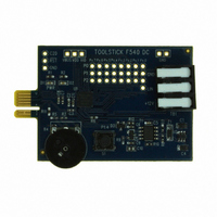
Manufacturer Part Number
TOOLSTICK540DC
Description
DAUGHTER CARD TOOLSTICK F540
Manufacturer
Silicon Laboratories Inc
Series
ToolStickr
Type
MCUr
Datasheets
1.TOOLSTICK540DC.pdf
(274 pages)
2.TOOLSTICK540DC.pdf
(16 pages)
3.TOOLSTICK540DC.pdf
(12 pages)
Specifications of TOOLSTICK540DC
Contents
Daughter Card
Processor To Be Evaluated
C8051F54x
Processor Series
C8051F54x
Interface Type
USB
Operating Supply Voltage
2.7 V to 3.6 V
Lead Free Status / RoHS Status
Lead free / RoHS Compliant
For Use With/related Products
C8051F54x
For Use With
336-1345 - TOOLSTICK BASE ADAPTER336-1182 - ADAPTER USB DEBUG FOR C8051FXXX
Lead Free Status / Rohs Status
Lead free / RoHS Compliant
Other names
336-1717


C8051F54x
18.4. Port I/O Initialization
Port I/O initialization consists of the following steps:
1. Select the input mode (analog or digital) for all Port pins, using the Port Input Mode register (PnMDIN).
2. Select the output mode (open-drain or push-pull) for all Port pins, using the Port Output Mode register
3. Select any pins to be skipped by the I/O Crossbar using the Port Skip registers (PnSKIP).
4. Assign Port pins to desired peripherals.
5. Enable the Crossbar (XBARE = 1).
All Port pins must be configured as either analog or digital inputs. Any pins to be used as Comparator or
ADC inputs should be configured as an analog inputs. When a pin is configured as an analog input, its
weak pullup, digital driver, and digital receiver are disabled. This process saves power and reduces noise
on the analog input. Pins configured as digital inputs may still be used by analog peripherals; however this
practice is not recommended.
Additionally, all analog input pins should be configured to be skipped by the Crossbar (accomplished by
setting the associated bits in PnSKIP). Port input mode is set in the PnMDIN register, where a 1 indicates a
digital input, and a 0 indicates an analog input. All pins default to digital inputs on reset. See SFR Definition
18.13 for the PnMDIN register details.
152
(PnMDOUT).
Port
Special
Function
Signals
PIN I/O
UART_TX
UART_RX
SCK
MISO
MOSI
NSS
SDA
SCL
CP0
CP0A
CP1
CP1A
SYSCLK
CEX0
CEX1
CEX2
CEX3
CEX4
CEX5
ECI
T0
T1
LIN_TX
LIN_RX
Figure 18.4. Crossbar Priority Decoder in Example Configuration
0
0
1
1
2
1
P0SKIP[0:7]
3
0
P0
4
0
5
1
6
0
7
0
0
0
1
0
2
0
P1SKIP[0:7]
Rev. 1.1
*NSS Is only pinned out in 4-wire SPI Mode
3
0
P1
4
0
5
0
6
0
7
0
0
0
1
0
2
0
P2SKIP[0:7]
P2.2-P2.7, P3.0 only available on
3
0
P2
the 32-pin packages
4
0
5
0
6
0
7
0
P3SKIP[0]
P3
0
0
Related parts for TOOLSTICK540DC
Image
Part Number
Description
Manufacturer
Datasheet
Request
R

Part Number:
Description:
KIT TOOL EVAL SYS IN A USB STICK
Manufacturer:
Silicon Laboratories Inc
Datasheet:

Part Number:
Description:
TOOLSTICK DEBUG ADAPTER
Manufacturer:
Silicon Laboratories Inc
Datasheet:

Part Number:
Description:
TOOLSTICK BASE ADAPTER
Manufacturer:
Silicon Laboratories Inc
Datasheet:

Part Number:
Description:
TOOLSTICK DAUGHTER CARD
Manufacturer:
Silicon Laboratories Inc
Datasheet:

Part Number:
Description:
TOOLSTICK DAUGHTER CARD
Manufacturer:
Silicon Laboratories Inc
Datasheet:

Part Number:
Description:
TOOLSTICK DAUGHTER CARD
Manufacturer:
Silicon Laboratories Inc
Datasheet:

Part Number:
Description:
TOOLSTICK PROGRAMMING ADAPTER
Manufacturer:
Silicon Laboratories Inc
Datasheet:

Part Number:
Description:
TOOLSTICK DAUGHTER CARD
Manufacturer:
Silicon Laboratories Inc
Datasheet:

Part Number:
Description:
KIT STARTER TOOLSTICK
Manufacturer:
Silicon Laboratories Inc
Datasheet:

Part Number:
Description:
KIT UNIVERSITY TOOLSTICK STARTER
Manufacturer:
Silicon Laboratories Inc
Datasheet:

Part Number:
Description:
DAUGHTER CARD TOOLSTICK F330
Manufacturer:
Silicon Laboratories Inc
Datasheet:

Part Number:
Description:
CARD DAUGHTER UNIVRSTY TOOLSTICK
Manufacturer:
Silicon Laboratories Inc
Datasheet:

Part Number:
Description:
DAUGHTER CARD TOOLSTICK F582
Manufacturer:
Silicon Laboratories Inc
Datasheet:

Part Number:
Description:
DAUGHTER CARD TOOLSTICK F500
Manufacturer:
Silicon Laboratories Inc
Datasheet:

Part Number:
Description:
DAUGHTER CARD TOOLSTICK F560
Manufacturer:
Silicon Laboratories Inc
Datasheet: