TOOLSTICK540DC Silicon Laboratories Inc, TOOLSTICK540DC Datasheet - Page 209
TOOLSTICK540DC
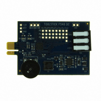
Manufacturer Part Number
TOOLSTICK540DC
Description
DAUGHTER CARD TOOLSTICK F540
Manufacturer
Silicon Laboratories Inc
Series
ToolStickr
Type
MCUr
Datasheets
1.TOOLSTICK540DC.pdf
(274 pages)
2.TOOLSTICK540DC.pdf
(16 pages)
3.TOOLSTICK540DC.pdf
(12 pages)
Specifications of TOOLSTICK540DC
Contents
Daughter Card
Processor To Be Evaluated
C8051F54x
Processor Series
C8051F54x
Interface Type
USB
Operating Supply Voltage
2.7 V to 3.6 V
Lead Free Status / RoHS Status
Lead free / RoHS Compliant
For Use With/related Products
C8051F54x
For Use With
336-1345 - TOOLSTICK BASE ADAPTER336-1182 - ADAPTER USB DEBUG FOR C8051FXXX
Lead Free Status / Rohs Status
Lead free / RoHS Compliant
Other names
336-1717


1. Clear RI0 to 0.
2. Read SBUF0.
3. Check RI0, and repeat at step 1 if RI0 is set to 1.
If the extra bit function is enabled (XBE0 = 1) and the parity function is disabled (PE0 = 0), the extra bit for
the oldest byte in the FIFO can be read from the RBX0 bit (SCON0.2). If the extra bit function is not
enabled, the value of the stop bit for the oldest FIFO byte will be presented in RBX0. When the parity func-
tion is enabled (PE0 = 1), hardware will check the received parity bit against the selected parity type
(selected with S0PT[1:0]) when receiving data. If a byte with parity error is received, the PERR0 flag will be
set to 1. This flag must be cleared by software. Note: when parity is enabled, the extra bit function is not
available.
21.3.3. Multiprocessor Communications
UART0 supports multiprocessor communication between a master processor and one or more slave pro-
cessors by special use of the extra data bit. When a master processor wants to transmit to one or more
slaves, it first sends an address byte to select the target(s). An address byte differs from a data byte in that
its extra bit is logic 1; in a data byte, the extra bit is always set to logic 0.
Setting the MCE0 bit (SMOD0.7) of a slave processor configures its UART such that when a stop bit is
received, the UART will generate an interrupt only if the extra bit is logic 1 (RBX0 = 1) signifying an
address byte has been received. In the UART interrupt handler, software will compare the received
address with the slave's own assigned address. If the addresses match, the slave will clear its MCE0 bit to
enable interrupts on the reception of the following data byte(s). Slaves that weren't addressed leave their
MCE0 bits set and do not generate interrupts on the reception of the following data bytes, thereby ignoring
the data. Once the entire message is received, the addressed slave resets its MCE0 bit to ignore all trans-
missions until it receives the next address byte.
Multiple addresses can be assigned to a single slave and/or a single address can be assigned to multiple
slaves, thereby enabling "broadcast" transmissions to more than one slave simultaneously. The master
processor can be configured to receive all transmissions or a protocol can be implemented such that the
master/slave role is temporarily reversed to enable half-duplex transmission between the original master
and slave(s).
RX
Master
Device
Figure 21.6. UART Multi-Processor Mode Interconnect Diagram
TX
RX
Device
Slave
TX
Rev. 1.1
RX
Device
Slave
TX
RX
Device
Slave
TX
C8051F54x
V+
209
Related parts for TOOLSTICK540DC
Image
Part Number
Description
Manufacturer
Datasheet
Request
R

Part Number:
Description:
KIT TOOL EVAL SYS IN A USB STICK
Manufacturer:
Silicon Laboratories Inc
Datasheet:

Part Number:
Description:
TOOLSTICK DEBUG ADAPTER
Manufacturer:
Silicon Laboratories Inc
Datasheet:

Part Number:
Description:
TOOLSTICK BASE ADAPTER
Manufacturer:
Silicon Laboratories Inc
Datasheet:

Part Number:
Description:
TOOLSTICK DAUGHTER CARD
Manufacturer:
Silicon Laboratories Inc
Datasheet:

Part Number:
Description:
TOOLSTICK DAUGHTER CARD
Manufacturer:
Silicon Laboratories Inc
Datasheet:

Part Number:
Description:
TOOLSTICK DAUGHTER CARD
Manufacturer:
Silicon Laboratories Inc
Datasheet:

Part Number:
Description:
TOOLSTICK PROGRAMMING ADAPTER
Manufacturer:
Silicon Laboratories Inc
Datasheet:

Part Number:
Description:
TOOLSTICK DAUGHTER CARD
Manufacturer:
Silicon Laboratories Inc
Datasheet:

Part Number:
Description:
KIT STARTER TOOLSTICK
Manufacturer:
Silicon Laboratories Inc
Datasheet:

Part Number:
Description:
KIT UNIVERSITY TOOLSTICK STARTER
Manufacturer:
Silicon Laboratories Inc
Datasheet:

Part Number:
Description:
DAUGHTER CARD TOOLSTICK F330
Manufacturer:
Silicon Laboratories Inc
Datasheet:

Part Number:
Description:
CARD DAUGHTER UNIVRSTY TOOLSTICK
Manufacturer:
Silicon Laboratories Inc
Datasheet:

Part Number:
Description:
DAUGHTER CARD TOOLSTICK F582
Manufacturer:
Silicon Laboratories Inc
Datasheet:

Part Number:
Description:
DAUGHTER CARD TOOLSTICK F500
Manufacturer:
Silicon Laboratories Inc
Datasheet:

Part Number:
Description:
DAUGHTER CARD TOOLSTICK F560
Manufacturer:
Silicon Laboratories Inc
Datasheet: