TOOLSTICK540DC Silicon Laboratories Inc, TOOLSTICK540DC Datasheet - Page 40
TOOLSTICK540DC
Manufacturer Part Number
TOOLSTICK540DC
Description
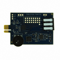
DAUGHTER CARD TOOLSTICK F540
Manufacturer
Silicon Laboratories Inc
Series
ToolStickr
Type
MCUr
Datasheets
1.TOOLSTICK540DC.pdf
(274 pages)
2.TOOLSTICK540DC.pdf
(16 pages)
3.TOOLSTICK540DC.pdf
(12 pages)
Specifications of TOOLSTICK540DC
Contents
Daughter Card
Processor To Be Evaluated
C8051F54x
Processor Series
C8051F54x
Interface Type
USB
Operating Supply Voltage
2.7 V to 3.6 V
Lead Free Status / RoHS Status
Lead free / RoHS Compliant
For Use With/related Products
C8051F54x
For Use With
336-1345 - TOOLSTICK BASE ADAPTER336-1182 - ADAPTER USB DEBUG FOR C8051FXXX
Lead Free Status / Rohs Status
Lead free / RoHS Compliant
Other names
336-1717


C8051F54x
SFR Definition 5.4. ADC0CF: ADC0 Configuration
SFR Address = 0xBC; SFR Page = 0x00
40
Name
Reset
7:3 AD0SC[4:0] ADC0 SAR Conversion Clock Period Bits.
2:1
Bit
Type
0
Bit
A0RPT[1:0] ADC0 Repeat Count
GAINEN
Name
7
1
SAR Conversion clock is derived from system clock by the following equation, where
AD0SC refers to the 5-bit value held in bits AD0SC4–0. SAR Conversion clock
requirements are given in the ADC specification table
BURSTEN = 0: FCLK is the current system clock
BURSTEN = 1: FCLK is a maximum of 30 MHz, independent of the current system
clock..
Note: Round up the result of the calculation for AD0SC
Controls the number of conversions taken and accumulated between ADC0 End of
Conversion (ADCINT) and ADC0 Window Comparator (ADCWINT) interrupts. A con-
vert start is required for each conversion unless Burst Mode is enabled. In Burst
Mode, a single convert start can initiate multiple self-timed conversions. Results in
both modes are accumulated in the ADC0H:ADC0L register. When AD0RPT1–0 are
set to a value other than '00', the AD0LJST bit in the ADC0CN register must be
set to '0' (right justified).
00: 1 conversion is performed.
01: 4 conversions are performed and accumulated.
10: 8 conversions are performed and accumulated.
11: 16 conversions are performed and accumulated.
Gain Enable Bit.
Controls the gain programming. Refer to Section “5.3. Selectable Gain” on page 35
for information about using this bit.
AD0SC
6
1
=
AD0SC[4:0]
-------------------- 1
CLK
R/W
FCLK
5
1
SAR
–
Rev. 1.1
4
1
Function
3
1
R/W
2
AD0RPT[1:0]
0
R/W
1
0
GAINEN
R/W
0
0
Related parts for TOOLSTICK540DC
Image
Part Number
Description
Manufacturer
Datasheet
Request
R

Part Number:
Description:
KIT TOOL EVAL SYS IN A USB STICK
Manufacturer:
Silicon Laboratories Inc
Datasheet:

Part Number:
Description:
TOOLSTICK DEBUG ADAPTER
Manufacturer:
Silicon Laboratories Inc
Datasheet:

Part Number:
Description:
TOOLSTICK BASE ADAPTER
Manufacturer:
Silicon Laboratories Inc
Datasheet:

Part Number:
Description:
TOOLSTICK DAUGHTER CARD
Manufacturer:
Silicon Laboratories Inc
Datasheet:

Part Number:
Description:
TOOLSTICK DAUGHTER CARD
Manufacturer:
Silicon Laboratories Inc
Datasheet:

Part Number:
Description:
TOOLSTICK DAUGHTER CARD
Manufacturer:
Silicon Laboratories Inc
Datasheet:

Part Number:
Description:
TOOLSTICK PROGRAMMING ADAPTER
Manufacturer:
Silicon Laboratories Inc
Datasheet:

Part Number:
Description:
TOOLSTICK DAUGHTER CARD
Manufacturer:
Silicon Laboratories Inc
Datasheet:

Part Number:
Description:
KIT STARTER TOOLSTICK
Manufacturer:
Silicon Laboratories Inc
Datasheet:

Part Number:
Description:
KIT UNIVERSITY TOOLSTICK STARTER
Manufacturer:
Silicon Laboratories Inc
Datasheet:

Part Number:
Description:
DAUGHTER CARD TOOLSTICK F330
Manufacturer:
Silicon Laboratories Inc
Datasheet:

Part Number:
Description:
CARD DAUGHTER UNIVRSTY TOOLSTICK
Manufacturer:
Silicon Laboratories Inc
Datasheet:

Part Number:
Description:
DAUGHTER CARD TOOLSTICK F582
Manufacturer:
Silicon Laboratories Inc
Datasheet:

Part Number:
Description:
DAUGHTER CARD TOOLSTICK F500
Manufacturer:
Silicon Laboratories Inc
Datasheet:

Part Number:
Description:
DAUGHTER CARD TOOLSTICK F560
Manufacturer:
Silicon Laboratories Inc
Datasheet: