TOOLSTICK540DC Silicon Laboratories Inc, TOOLSTICK540DC Datasheet - Page 148
TOOLSTICK540DC
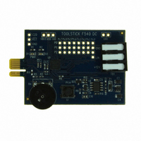
Manufacturer Part Number
TOOLSTICK540DC
Description
DAUGHTER CARD TOOLSTICK F540
Manufacturer
Silicon Laboratories Inc
Series
ToolStickr
Type
MCUr
Datasheets
1.TOOLSTICK540DC.pdf
(274 pages)
2.TOOLSTICK540DC.pdf
(16 pages)
3.TOOLSTICK540DC.pdf
(12 pages)
Specifications of TOOLSTICK540DC
Contents
Daughter Card
Processor To Be Evaluated
C8051F54x
Processor Series
C8051F54x
Interface Type
USB
Operating Supply Voltage
2.7 V to 3.6 V
Lead Free Status / RoHS Status
Lead free / RoHS Compliant
For Use With/related Products
C8051F54x
For Use With
336-1345 - TOOLSTICK BASE ADAPTER336-1182 - ADAPTER USB DEBUG FOR C8051FXXX
Lead Free Status / Rohs Status
Lead free / RoHS Compliant
Other names
336-1717


C8051F54x
18.1. Port I/O Modes of Operation
Port pins P0.0–P3.0 use the Port I/O cell shown in Figure 18.2. Each Port I/O cell can be configured by
software for analog I/O or digital I/O using the PnMDIN registers. On reset, all Port I/O cells default to a
high impedance state with weak pull-ups enabled until the Crossbar is enabled (XBARE = 1).
18.1.1. Port Pins Configured for Analog I/O
Any pins to be used as Comparator or ADC inputs, external oscillator inputs, or VREF should be config-
ured for analog I/O (PnMDIN.n = 0). When a pin is configured for analog I/O, its weak pullup, digital driver,
and digital receiver are disabled. Port pins configured for analog I/O will always read back a value of 0.
Configuring pins as analog I/O saves power and isolates the Port pin from digital interference. Port pins
configured as digital inputs may still be used by analog peripherals; however, this practice is not recom-
mended and may result in measurement errors.
18.1.2. Port Pins Configured For Digital I/O
Any pins to be used by digital peripherals (UART, SPI, SMBus, etc.), external digital event capture func-
tions, or as GPIO should be configured as digital I/O (PnMDIN.n = 1). For digital I/O pins, one of two output
modes (push-pull or open-drain) must be selected using the PnMDOUT registers.
Push-pull outputs (PnMDOUT.n = 1) drive the Port pad to the VIO or GND supply rails based on the output
logic value of the Port pin. Open-drain outputs have the high side driver disabled; therefore, they only drive
the Port pad to GND when the output logic value is 0 and become high impedance inputs (both high low
drivers turned off) when the output logic value is 1.
When a digital I/O cell is placed in the high impedance state, a weak pull-up transistor pulls the Port pad to
the VIO supply voltage to ensure the digital input is at a defined logic state. Weak pull-ups are disabled
when the I/O cell is driven to GND to minimize power consumption and may be globally disabled by setting
WEAKPUD to 1. The user should ensure that digital I/O are always internally or externally pulled or driven
to a valid logic state to minimize power consumption. Port pins configured for digital I/O always read back
the logic state of the Port pad, regardless of the output logic value of the Port pin.
148
WEAKPUD
(Weak Pull-Up Disable)
Px.x – Output
Logic Value
(Port Latch or
Crossbar)
PxMDOUT.x
(1 for push-pull)
(0 for open-drain)
XBARE
(Crossbar
Enable)
Px.x – Input Logic Value
(Reads 0 when pin is configured as an analog I/O)
To/From Analog
Peripheral
PxMDIN.x
(1 for digital)
(0 for analog)
Figure 18.2. Port I/O Cell Block Diagram
Rev. 1.1
VIO
GND
VIO
(WEAK)
PORT
PAD
Related parts for TOOLSTICK540DC
Image
Part Number
Description
Manufacturer
Datasheet
Request
R

Part Number:
Description:
KIT TOOL EVAL SYS IN A USB STICK
Manufacturer:
Silicon Laboratories Inc
Datasheet:

Part Number:
Description:
TOOLSTICK DEBUG ADAPTER
Manufacturer:
Silicon Laboratories Inc
Datasheet:

Part Number:
Description:
TOOLSTICK BASE ADAPTER
Manufacturer:
Silicon Laboratories Inc
Datasheet:

Part Number:
Description:
TOOLSTICK DAUGHTER CARD
Manufacturer:
Silicon Laboratories Inc
Datasheet:

Part Number:
Description:
TOOLSTICK DAUGHTER CARD
Manufacturer:
Silicon Laboratories Inc
Datasheet:

Part Number:
Description:
TOOLSTICK DAUGHTER CARD
Manufacturer:
Silicon Laboratories Inc
Datasheet:

Part Number:
Description:
TOOLSTICK PROGRAMMING ADAPTER
Manufacturer:
Silicon Laboratories Inc
Datasheet:

Part Number:
Description:
TOOLSTICK DAUGHTER CARD
Manufacturer:
Silicon Laboratories Inc
Datasheet:

Part Number:
Description:
KIT STARTER TOOLSTICK
Manufacturer:
Silicon Laboratories Inc
Datasheet:

Part Number:
Description:
KIT UNIVERSITY TOOLSTICK STARTER
Manufacturer:
Silicon Laboratories Inc
Datasheet:

Part Number:
Description:
DAUGHTER CARD TOOLSTICK F330
Manufacturer:
Silicon Laboratories Inc
Datasheet:

Part Number:
Description:
CARD DAUGHTER UNIVRSTY TOOLSTICK
Manufacturer:
Silicon Laboratories Inc
Datasheet:

Part Number:
Description:
DAUGHTER CARD TOOLSTICK F582
Manufacturer:
Silicon Laboratories Inc
Datasheet:

Part Number:
Description:
DAUGHTER CARD TOOLSTICK F500
Manufacturer:
Silicon Laboratories Inc
Datasheet:

Part Number:
Description:
DAUGHTER CARD TOOLSTICK F560
Manufacturer:
Silicon Laboratories Inc
Datasheet: