C8051F560-TB Silicon Laboratories Inc, C8051F560-TB Datasheet - Page 137
C8051F560-TB
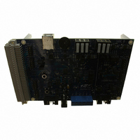
Manufacturer Part Number
C8051F560-TB
Description
BOARD PROTOTYPE W/C8051F560
Manufacturer
Silicon Laboratories Inc
Type
MCUr
Datasheet
1.TOOLSTICK560DC.pdf
(302 pages)
Specifications of C8051F560-TB
Contents
Board
Processor To Be Evaluated
C8051F56x
Processor Series
C8051F56x
Interface Type
USB
Maximum Operating Temperature
+ 125 C
Minimum Operating Temperature
- 40 C
Operating Supply Voltage
1.8 V to 5.25 V
Lead Free Status / RoHS Status
Lead free / RoHS Compliant
For Use With/related Products
C8051F55x, C8051F56x, C8051F57x
For Use With
336-1691 - KIT DEVELOPMENT FOR C8051F560
Lead Free Status / Rohs Status
Lead free / RoHS Compliant
Other names
336-1694


16.1. Power-On Reset
During power-up, the device is held in a reset state and the RST pin is driven low until V
V
increases (V
power-on and V
On exit from a power-on reset, the PORSF flag (RSTSRC.1) is set by hardware to logic 1. When PORSF is
set, all of the other reset flags in the RSTSRC Register are indeterminate (PORSF is cleared by all other
resets). Since all resets cause program execution to begin at the same location (0x0000) software can
read the PORSF flag to determine if a power-up was the cause of reset. The content of internal data mem-
ory should be assumed to be undefined after a power-on reset. The V
power-on reset.
16.2. Power-Fail Reset/V
When a power-down transition or power irregularity causes V
monitor will drive the RST pin low and hold the CIP-51 in a reset state (see Figure 16.2). When V
to a level above V
memory contents are not altered by the power-fail reset, it is impossible to determine if V
the level required for data retention. If the PORSF flag reads 1, the data may no longer be valid. The V
monitor is enabled after power-on resets. Its defined state (enabled/disabled) is not altered by any other
reset source. For example, if the V
V
monitor must be enabled to the higher setting (VDMLVL = 1) and selected as a reset source if soft-
ware contains routines which erase or write Flash memory. If the V
set to the high level, any erase or write performed on Flash memory will cause a Flash Error device
reset.
RST
DD
. A delay occurs before the device is released from reset; the delay decreases as the V
monitor will still be disabled after the reset. To protect the integrity of Flash contents, the V
DD
Logic HIGH
Logic LOW
DD
ramp time is defined as how fast V
2.45
2.25
2.0
1.0
RST
monitor reset timing.
, the CIP-51 will be released from the reset state. Note that even though internal data
Figure 16.2. Power-On and V
/RST
V
RST
DD
DD
Monitor
Power-On
monitor is disabled by code and a software reset is performed, the
Reset
T
PORDelay
Rev. 1.1
DD
DD
ramps from 0 V to V
Monitor Reset Timing
DD
C8051F55x/56x/57x
to drop below V
Monitor
Reset
VDD
DD
DD
monitor is enabled following a
monitor is not enabled and
RST
). Figure 16.2. plots the
RST
VDD
, the power supply
DD
DD
dropped below
t
settles above
DD
DD
ramp time
returns
137
DD
DD
Related parts for C8051F560-TB
Image
Part Number
Description
Manufacturer
Datasheet
Request
R

Part Number:
Description:
SMD/C°/SINGLE-ENDED OUTPUT SILICON OSCILLATOR
Manufacturer:
Silicon Laboratories Inc
Part Number:
Description:
Manufacturer:
Silicon Laboratories Inc
Datasheet:
Part Number:
Description:
N/A N/A/SI4010 AES KEYFOB DEMO WITH LCD RX
Manufacturer:
Silicon Laboratories Inc
Datasheet:
Part Number:
Description:
N/A N/A/SI4010 SIMPLIFIED KEY FOB DEMO WITH LED RX
Manufacturer:
Silicon Laboratories Inc
Datasheet:
Part Number:
Description:
N/A/-40 TO 85 OC/EZLINK MODULE; F930/4432 HIGH BAND (REV E/B1)
Manufacturer:
Silicon Laboratories Inc
Part Number:
Description:
EZLink Module; F930/4432 Low Band (rev e/B1)
Manufacturer:
Silicon Laboratories Inc
Part Number:
Description:
I°/4460 10 DBM RADIO TEST CARD 434 MHZ
Manufacturer:
Silicon Laboratories Inc
Part Number:
Description:
I°/4461 14 DBM RADIO TEST CARD 868 MHZ
Manufacturer:
Silicon Laboratories Inc
Part Number:
Description:
I°/4463 20 DBM RFSWITCH RADIO TEST CARD 460 MHZ
Manufacturer:
Silicon Laboratories Inc
Part Number:
Description:
I°/4463 20 DBM RADIO TEST CARD 868 MHZ
Manufacturer:
Silicon Laboratories Inc
Part Number:
Description:
I°/4463 27 DBM RADIO TEST CARD 868 MHZ
Manufacturer:
Silicon Laboratories Inc
Part Number:
Description:
I°/4463 SKYWORKS 30 DBM RADIO TEST CARD 915 MHZ
Manufacturer:
Silicon Laboratories Inc
Part Number:
Description:
N/A N/A/-40 TO 85 OC/4463 RFMD 30 DBM RADIO TEST CARD 915 MHZ
Manufacturer:
Silicon Laboratories Inc
Part Number:
Description:
I°/4463 20 DBM RADIO TEST CARD 169 MHZ
Manufacturer:
Silicon Laboratories Inc