C8051F560-TB Silicon Laboratories Inc, C8051F560-TB Datasheet - Page 278
C8051F560-TB
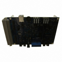
Manufacturer Part Number
C8051F560-TB
Description
BOARD PROTOTYPE W/C8051F560
Manufacturer
Silicon Laboratories Inc
Type
MCUr
Datasheet
1.TOOLSTICK560DC.pdf
(302 pages)
Specifications of C8051F560-TB
Contents
Board
Processor To Be Evaluated
C8051F56x
Processor Series
C8051F56x
Interface Type
USB
Maximum Operating Temperature
+ 125 C
Minimum Operating Temperature
- 40 C
Operating Supply Voltage
1.8 V to 5.25 V
Lead Free Status / RoHS Status
Lead free / RoHS Compliant
For Use With/related Products
C8051F55x, C8051F56x, C8051F57x
For Use With
336-1691 - KIT DEVELOPMENT FOR C8051F560
Lead Free Status / Rohs Status
Lead free / RoHS Compliant
Other names
336-1694


C8051F55x/56x/57x
26.1. PCA Counter/Timer
The 16-bit PCA counter/timer consists of two 8-bit SFRs: PCA0L and PCA0H. PCA0H is the high byte
(MSB) of the 16-bit counter/timer and PCA0L is the low byte (LSB). Reading PCA0L automatically latches
the value of PCA0H into a “snapshot” register; the following PCA0H read accesses this “snapshot” register.
Reading the PCA0L Register first guarantees an accurate reading of the entire 16-bit PCA0 counter.
Reading PCA0H or PCA0L does not disturb the counter operation. The CPS[2:0] bits in the PCA0MD reg-
ister select the timebase for the counter/timer as shown in Table 26.1.
When the counter/timer overflows from 0xFFFF to 0x0000, the Counter Overflow Flag (CF) in PCA0MD is
set to logic 1 and an interrupt request is generated if CF interrupts are enabled. Setting the ECF bit in
PCA0MD to logic 1 enables the CF flag to generate an interrupt request. The CF bit is not automatically
cleared by hardware when the CPU vectors to the interrupt service routine, and must be cleared by soft-
ware. Clearing the CIDL bit in the PCA0MD register allows the PCA to continue normal operation while the
CPU is in Idle mode.
278
SYSCLK/12
SYSCLK/4
Timer 0 Overflow
ECI
SYSCLK
External Clock/8
*Note: External oscillator source divided by 8 is synchronized with the system clock.
CPS2
0
0
0
0
1
1
1
C
D
L
I
W
D
E
T
PCA0MD
W
D
C
K
L
CPS1
C
P
S
2
000
001
010
011
100
101
C
P
S
1
0
0
1
1
0
0
1
C
P
S
0
C
E
F
Figure 26.2. PCA Counter/Timer Block Diagram
IDLE
CPS0
Table 26.1. PCA Timebase Input Options
C
0
1
0
1
0
1
x
F
C
R
PCA0CN
C
C
F
5
C
C
F
4
C
C
F
3
System clock divided by 12.
System clock divided by 4.
Timer 0 overflow.
High-to-low transitions on ECI (max rate = system clock divided
by 4).
System clock.
External oscillator source divided by 8.
Reserved.
C
C
F
2
C
C
F
1
C
C
F
0
Rev. 1.1
0
1
PCA0L
read
Snapshot
Register
PCA0H
Timebase
PCA0L
*
To SFR Bus
To PCA Modules
Overflow
CF
To PCA Interrupt System
Related parts for C8051F560-TB
Image
Part Number
Description
Manufacturer
Datasheet
Request
R

Part Number:
Description:
SMD/C°/SINGLE-ENDED OUTPUT SILICON OSCILLATOR
Manufacturer:
Silicon Laboratories Inc
Part Number:
Description:
Manufacturer:
Silicon Laboratories Inc
Datasheet:
Part Number:
Description:
N/A N/A/SI4010 AES KEYFOB DEMO WITH LCD RX
Manufacturer:
Silicon Laboratories Inc
Datasheet:
Part Number:
Description:
N/A N/A/SI4010 SIMPLIFIED KEY FOB DEMO WITH LED RX
Manufacturer:
Silicon Laboratories Inc
Datasheet:
Part Number:
Description:
N/A/-40 TO 85 OC/EZLINK MODULE; F930/4432 HIGH BAND (REV E/B1)
Manufacturer:
Silicon Laboratories Inc
Part Number:
Description:
EZLink Module; F930/4432 Low Band (rev e/B1)
Manufacturer:
Silicon Laboratories Inc
Part Number:
Description:
I°/4460 10 DBM RADIO TEST CARD 434 MHZ
Manufacturer:
Silicon Laboratories Inc
Part Number:
Description:
I°/4461 14 DBM RADIO TEST CARD 868 MHZ
Manufacturer:
Silicon Laboratories Inc
Part Number:
Description:
I°/4463 20 DBM RFSWITCH RADIO TEST CARD 460 MHZ
Manufacturer:
Silicon Laboratories Inc
Part Number:
Description:
I°/4463 20 DBM RADIO TEST CARD 868 MHZ
Manufacturer:
Silicon Laboratories Inc
Part Number:
Description:
I°/4463 27 DBM RADIO TEST CARD 868 MHZ
Manufacturer:
Silicon Laboratories Inc
Part Number:
Description:
I°/4463 SKYWORKS 30 DBM RADIO TEST CARD 915 MHZ
Manufacturer:
Silicon Laboratories Inc
Part Number:
Description:
N/A N/A/-40 TO 85 OC/4463 RFMD 30 DBM RADIO TEST CARD 915 MHZ
Manufacturer:
Silicon Laboratories Inc
Part Number:
Description:
I°/4463 20 DBM RADIO TEST CARD 169 MHZ
Manufacturer:
Silicon Laboratories Inc