C8051F560-TB Silicon Laboratories Inc, C8051F560-TB Datasheet - Page 4
C8051F560-TB
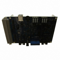
Manufacturer Part Number
C8051F560-TB
Description
BOARD PROTOTYPE W/C8051F560
Manufacturer
Silicon Laboratories Inc
Type
MCUr
Datasheet
1.TOOLSTICK560DC.pdf
(302 pages)
Specifications of C8051F560-TB
Contents
Board
Processor To Be Evaluated
C8051F56x
Processor Series
C8051F56x
Interface Type
USB
Maximum Operating Temperature
+ 125 C
Minimum Operating Temperature
- 40 C
Operating Supply Voltage
1.8 V to 5.25 V
Lead Free Status / RoHS Status
Lead free / RoHS Compliant
For Use With/related Products
C8051F55x, C8051F56x, C8051F57x
For Use With
336-1691 - KIT DEVELOPMENT FOR C8051F560
Lead Free Status / Rohs Status
Lead free / RoHS Compliant
Other names
336-1694


C8051F55x/56x/57x
13. Interrupts .............................................................................................................. 112
14. Flash Memory....................................................................................................... 124
15. Power Management Modes................................................................................. 133
16. Reset Sources ...................................................................................................... 136
17. External Data Memory Interface and On-Chip XRAM ....................................... 142
4
12.2. Interrupts and SFR Paging .............................................................................. 95
12.3. SFR Page Stack Example ............................................................................... 97
13.1. MCU Interrupt Sources and Vectors.............................................................. 112
13.2. Interrupt Register Descriptions ...................................................................... 115
13.3. External Interrupts INT0 and INT1................................................................. 122
14.1. Programming The Flash Memory .................................................................. 124
14.2. Non-volatile Data Storage ............................................................................. 126
14.3. Security Options ............................................................................................ 126
14.4. Flash Write and Erase Guidelines ................................................................. 128
15.1. Idle Mode....................................................................................................... 133
15.2. Stop Mode ..................................................................................................... 134
15.3. Suspend Mode .............................................................................................. 134
16.1. Power-On Reset ............................................................................................ 137
16.2. Power-Fail Reset/VDD Monitor ..................................................................... 137
16.3. External Reset ............................................................................................... 139
16.4. Missing Clock Detector Reset ....................................................................... 139
16.5. Comparator0 Reset ....................................................................................... 140
16.6. PCA Watchdog Timer Reset ......................................................................... 140
16.7. Flash Error Reset .......................................................................................... 140
16.8. Software Reset .............................................................................................. 140
17.1. Accessing XRAM........................................................................................... 142
17.2. Configuring the External Memory Interface ................................................... 143
17.3. Port Configuration.......................................................................................... 143
17.4. Multiplexed Mode .......................................................................................... 147
17.5. Memory Mode Selection................................................................................ 148
13.1.1. Interrupt Priorities.................................................................................. 113
13.1.2. Interrupt Latency ................................................................................... 113
14.1.1. Flash Lock and Key Functions .............................................................. 124
14.1.2. Flash Erase Procedure ......................................................................... 124
14.1.3. Flash Write Procedure .......................................................................... 125
14.1.4. Flash Write Optimization ....................................................................... 125
14.4.1. V
14.4.2. PSWE Maintenance .............................................................................. 128
14.4.3. System Clock ........................................................................................ 129
17.1.1. 16-Bit MOVX Example .......................................................................... 142
17.1.2. 8-Bit MOVX Example ............................................................................ 142
17.5.1. Internal XRAM Only .............................................................................. 148
17.5.2. Split Mode without Bank Select............................................................. 148
17.5.3. Split Mode with Bank Select.................................................................. 149
17.5.4. External Only......................................................................................... 149
DD
Maintenance and the V
Rev. 1.1
DD
monitor ................................................ 128
Related parts for C8051F560-TB
Image
Part Number
Description
Manufacturer
Datasheet
Request
R

Part Number:
Description:
SMD/C°/SINGLE-ENDED OUTPUT SILICON OSCILLATOR
Manufacturer:
Silicon Laboratories Inc
Part Number:
Description:
Manufacturer:
Silicon Laboratories Inc
Datasheet:
Part Number:
Description:
N/A N/A/SI4010 AES KEYFOB DEMO WITH LCD RX
Manufacturer:
Silicon Laboratories Inc
Datasheet:
Part Number:
Description:
N/A N/A/SI4010 SIMPLIFIED KEY FOB DEMO WITH LED RX
Manufacturer:
Silicon Laboratories Inc
Datasheet:
Part Number:
Description:
N/A/-40 TO 85 OC/EZLINK MODULE; F930/4432 HIGH BAND (REV E/B1)
Manufacturer:
Silicon Laboratories Inc
Part Number:
Description:
EZLink Module; F930/4432 Low Band (rev e/B1)
Manufacturer:
Silicon Laboratories Inc
Part Number:
Description:
I°/4460 10 DBM RADIO TEST CARD 434 MHZ
Manufacturer:
Silicon Laboratories Inc
Part Number:
Description:
I°/4461 14 DBM RADIO TEST CARD 868 MHZ
Manufacturer:
Silicon Laboratories Inc
Part Number:
Description:
I°/4463 20 DBM RFSWITCH RADIO TEST CARD 460 MHZ
Manufacturer:
Silicon Laboratories Inc
Part Number:
Description:
I°/4463 20 DBM RADIO TEST CARD 868 MHZ
Manufacturer:
Silicon Laboratories Inc
Part Number:
Description:
I°/4463 27 DBM RADIO TEST CARD 868 MHZ
Manufacturer:
Silicon Laboratories Inc
Part Number:
Description:
I°/4463 SKYWORKS 30 DBM RADIO TEST CARD 915 MHZ
Manufacturer:
Silicon Laboratories Inc
Part Number:
Description:
N/A N/A/-40 TO 85 OC/4463 RFMD 30 DBM RADIO TEST CARD 915 MHZ
Manufacturer:
Silicon Laboratories Inc
Part Number:
Description:
I°/4463 20 DBM RADIO TEST CARD 169 MHZ
Manufacturer:
Silicon Laboratories Inc