STEVAL-IFS001V1 STMicroelectronics, STEVAL-IFS001V1 Datasheet - Page 19
STEVAL-IFS001V1
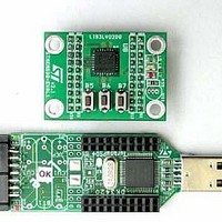
Manufacturer Part Number
STEVAL-IFS001V1
Description
EVAL BOARD 3AXIS MEMS ACCELLRMTR
Manufacturer
STMicroelectronics
Series
MEMSr
Datasheets
1.STEVAL-IFS001V1.pdf
(42 pages)
2.STEVAL-IFS001V1.pdf
(14 pages)
3.STEVAL-IFS001V1.pdf
(4 pages)
4.STEVAL-IFS001V1.pdf
(14 pages)
Specifications of STEVAL-IFS001V1
Design Resources
STEVAL-IFS001V1 Gerber Files STEVAL-IFS001V1 Schematic STEVAL-IFS001V1 Bill of Material
Sensor Type
Accelerometer, 3 Axis
Sensing Range
±2g, 6g
Interface
I²C, SPI
Sensitivity
1024 LSb/g
Voltage - Supply
2.16 V ~ 3.6 V
Embedded
Yes, MCU, 8-Bit
Utilized Ic / Part
LIS3LV02DQ
Processor To Be Evaluated
LIS3LV02DQ
Interface Type
USB
Lead Free Status / RoHS Status
Contains lead / RoHS non-compliant
Other names
497-5069
Available stocks
Company
Part Number
Manufacturer
Quantity
Price


LIS3LV02DQ
5.2
function, it can hold the clock line, SCL LOW to force the transmitter into a wait state. Data
transfer only continues when the receiver is ready for another byte and releases the data line. If
a slave receiver doesn’t acknowledge the slave address (i.e. it is not able to receive because it
is performing some real time function) the data line must be left HIGH by the slave. The Master
can then abort the transfer. A LOW to HIGH transition on the SDA line while the SCL line is
HIGH is defined as a STOP condition. Each data transfer must be terminated by the generation
of a STOP (SP) condition.
In order to read multiple bytes, it is necessary to assert the most significant bit of the sub-
address field. In other words, SUB(7) must be equal to 1 while SUB(6-0) represents the
address of first register to read.
In the presented communication format MAK is Master Acknowledge and NMAK is No Master
Acknowledge.
SPI Bus Interface
The LIS3LV02DQ SPI is a bus slave. The SPI allows to write and read the registers of the
device.
The Serial Interface interacts with the outside world with 4 wires: CS, SPC, SDI and SDO.
Figure 4.
CS is the Serial Port Enable and it is controlled by the SPI master. It goes low at the start of the
transmission and goes back high at the end. SPC is the Serial Port Clock and it is controlled by
the SPI master. It is stopped high when CS is high (no transmission). SDI and SDO are
respectively the Serial Port Data Input and Output. Those lines are driven at the falling edge of
SPC and should be captured at the rising edge of SPC.
Both the Read Register and Write Register commands are completed in 16 clock pulses or in
multiple of 8 in case of multiple byte read/write. Bit duration is the time between two falling
edges of SPC. The first bit (bit 0) starts at the first falling edge of SPC after the falling edge of
CS while the last bit (bit 15, bit 23, ...) starts at the last falling edge of SPC just before the rising
edge of CS.
bit 0 : RW bit. When 0, the data DI(7:0) is written into the device. When 1, the data DO(7:0) from
the device is read. In latter case, the chip will drive SDO at the start of bit 8.
bit 1 : MS bit. When 0, the address will remain unchanged in multiple read/write commands.
When 1, the address will be auto incremented in multiple read/write commands.
bit 2-7 : address AD(5:0). This is the address field of the indexed register.
SDO
SPC
SDI
CS
Read & write protocol
RW
MS
AD5 AD4 AD3 AD2 AD1 AD0
CD00047926
DO7 DO6 DO5 DO4 DO3 DO2 DO1 DO0
DI7 DI6 DI5 DI4 DI3 DI2 DI1 DI0
5 Digital Interfaces
19/42
Related parts for STEVAL-IFS001V1
Image
Part Number
Description
Manufacturer
Datasheet
Request
R

Part Number:
Description:
BOARD EVAL SPZB260 MOD FOR STR9
Manufacturer:
STMicroelectronics
Datasheet:

Part Number:
Description:
BOARD EVAL EXTENSION SN250
Manufacturer:
STMicroelectronics
Datasheet:

Part Number:
Description:
BOARD EVAL AB-54003L-512
Manufacturer:
STMicroelectronics
Datasheet:

Part Number:
Description:
BOARD REF DESIGN RF DMOS PWR AMP
Manufacturer:
STMicroelectronics
Datasheet:

Part Number:
Description:
BOARD EVAL PWR AMP AB-84008L-470
Manufacturer:
STMicroelectronics
Datasheet:

Part Number:
Description:
BOARD EVAL FOR STM32F103XX
Manufacturer:
STMicroelectronics
Datasheet:

Part Number:
Description:
BOARD EVAL AB-54003L-512
Manufacturer:
STMicroelectronics
Datasheet:

Part Number:
Description:
BOARD SMART PLUG STM32 SPZB260PR
Manufacturer:
STMicroelectronics
Datasheet:

Part Number:
Description:
BOARD DEMO BLUETOOTH SPBT2532C2
Manufacturer:
STMicroelectronics
Datasheet:
Part Number:
Description:
ZIGBEE USB DONGLE EVAL KIT
Manufacturer:
STMicroelectronics
Datasheet:
Part Number:
Description:
STMicroelectronics [RIPPLE-CARRY BINARY COUNTER/DIVIDERS]
Manufacturer:
STMicroelectronics
Datasheet:
Part Number:
Description:
STMicroelectronics [LIQUID-CRYSTAL DISPLAY DRIVERS]
Manufacturer:
STMicroelectronics
Datasheet:

Part Number:
Description:
BOARD EVAL FOR MEMS SENSORS
Manufacturer:
STMicroelectronics
Datasheet: