STEVAL-IFS001V1 STMicroelectronics, STEVAL-IFS001V1 Datasheet - Page 27
STEVAL-IFS001V1
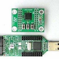
Manufacturer Part Number
STEVAL-IFS001V1
Description
EVAL BOARD 3AXIS MEMS ACCELLRMTR
Manufacturer
STMicroelectronics
Series
MEMSr
Datasheets
1.STEVAL-IFS001V1.pdf
(42 pages)
2.STEVAL-IFS001V1.pdf
(14 pages)
3.STEVAL-IFS001V1.pdf
(4 pages)
4.STEVAL-IFS001V1.pdf
(14 pages)
Specifications of STEVAL-IFS001V1
Design Resources
STEVAL-IFS001V1 Gerber Files STEVAL-IFS001V1 Schematic STEVAL-IFS001V1 Bill of Material
Sensor Type
Accelerometer, 3 Axis
Sensing Range
±2g, 6g
Interface
I²C, SPI
Sensitivity
1024 LSb/g
Voltage - Supply
2.16 V ~ 3.6 V
Embedded
Yes, MCU, 8-Bit
Utilized Ic / Part
LIS3LV02DQ
Processor To Be Evaluated
LIS3LV02DQ
Interface Type
USB
Lead Free Status / RoHS Status
Contains lead / RoHS non-compliant
Other names
497-5069
Available stocks
Company
Part Number
Manufacturer
Quantity
Price


LIS3LV02DQ
7.9
ST bit is used to activate the self test function. When the bit is set to one, an output change will
occur to the device outputs (refer to table 2 and 3 for specification) thus allowing to check the
functionality of the whole measurement chain.
Zen bit enables the Z-axis measurement channel when set to 1. The default value is 1.
Yen bit enables the Y-axis measurement channel when set to 1. The default value is 1.
Xen bit enables the X-axis measurement channel when set to 1. The default value is 1.
CTRL_REG2 (21h)
FS bit is used to select Full Scale value. After the device power-up the default full scale value is
+/-2g. In order to obtain a +/-6g full scale it is necessary to set FS bit to ‘1’.
BDU bit is used to inhibit output registers update until both upper and lower register parts are
read. In default mode (BDU= ‘0’) the output register values are updated continuously. If for any
reason it is not sure to read faster than output data rate it is recommended to set BDU bit to ‘1’.
In this way the content of output registers is not updated until both MSB and LSB are read
avoiding to read values related to different sample time.
BLE bit is used to select Big Endian or Little Endian representation for output registers. In Big
Endian’s one MSB acceleration value is located at addresses 28h (X-axis), 2Ah (Y-axis) and
2Ch (Z-axis) while LSB acceleration value is located at addresses 29h (X-axis), 2Bh (Y-axis)
and 2Dh (Z-axis). In Little Endian representation (Default, BLE=‘0‘) the order is inverted (refer
to data register description for more details).
BOOT bit is used to refresh the content of internal registers stored in the flash memory block.
At the device power up the content of the flash memory block is transferred to the internal
registers related to trimming functions to permit a good behavior of the device itself. If for any
reason the content of trimming registers was changed it is sufficient to use this bit to restore
correct values. When BOOT bit is set to ‘1’ the content of internal flash is copied inside
corresponding internal registers and it is used to calibrate the device. These values are factory
FS
BDU
BLE
BOOT
IEN
DRDY
SIM
DAS
Full Scale selection
(0: ±2g; 1: ±6g)
Block Data Update
(0: continuous update; 1: output registers not updated until MSB and LSB reading)
Big/Little Endian selection
(0: little endian; 1: big endian)
Reboot memory content
Interrupt ENable
(0: data ready on RDY pad; 1: int req on RDY pad)
Enable Data-Ready generation
SPI Serial Interface Mode selection
(0: 4-wire interface; 1: 3-wire interface)
Data Alignment Selection
(0: 12 bit right justified; 1: 16 bit left justified)
FS
BDU
BLE
CD00047926
BOOT
IEN
DRDY
SIM
DAS
7 Register Description
27/42
Related parts for STEVAL-IFS001V1
Image
Part Number
Description
Manufacturer
Datasheet
Request
R

Part Number:
Description:
BOARD EVAL SPZB260 MOD FOR STR9
Manufacturer:
STMicroelectronics
Datasheet:

Part Number:
Description:
BOARD EVAL EXTENSION SN250
Manufacturer:
STMicroelectronics
Datasheet:

Part Number:
Description:
BOARD EVAL AB-54003L-512
Manufacturer:
STMicroelectronics
Datasheet:

Part Number:
Description:
BOARD REF DESIGN RF DMOS PWR AMP
Manufacturer:
STMicroelectronics
Datasheet:

Part Number:
Description:
BOARD EVAL PWR AMP AB-84008L-470
Manufacturer:
STMicroelectronics
Datasheet:

Part Number:
Description:
BOARD EVAL FOR STM32F103XX
Manufacturer:
STMicroelectronics
Datasheet:

Part Number:
Description:
BOARD EVAL AB-54003L-512
Manufacturer:
STMicroelectronics
Datasheet:

Part Number:
Description:
BOARD SMART PLUG STM32 SPZB260PR
Manufacturer:
STMicroelectronics
Datasheet:

Part Number:
Description:
BOARD DEMO BLUETOOTH SPBT2532C2
Manufacturer:
STMicroelectronics
Datasheet:
Part Number:
Description:
ZIGBEE USB DONGLE EVAL KIT
Manufacturer:
STMicroelectronics
Datasheet:
Part Number:
Description:
STMicroelectronics [RIPPLE-CARRY BINARY COUNTER/DIVIDERS]
Manufacturer:
STMicroelectronics
Datasheet:
Part Number:
Description:
STMicroelectronics [LIQUID-CRYSTAL DISPLAY DRIVERS]
Manufacturer:
STMicroelectronics
Datasheet:

Part Number:
Description:
BOARD EVAL FOR MEMS SENSORS
Manufacturer:
STMicroelectronics
Datasheet: