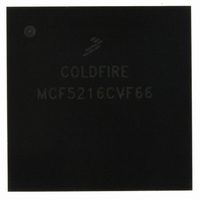
MCF5216CVF66 Freescale Semiconductor, MCF5216CVF66 Datasheet - Page 126

MCF5216CVF66
Manufacturer Part Number
MCF5216CVF66
Description
IC MPU 32BIT COLDF 256-MAPBGA
Manufacturer
Freescale Semiconductor
Series
MCF521xr
Datasheet
1.MCF5216CVM66J.pdf
(766 pages)
Specifications of MCF5216CVF66
Core Processor
Coldfire V2
Core Size
32-Bit
Speed
66MHz
Connectivity
CAN, EBI/EMI, I²C, SPI, UART/USART
Peripherals
DMA, LVD, POR, PWM, WDT
Number Of I /o
142
Program Memory Size
512KB (512K x 8)
Program Memory Type
FLASH
Ram Size
64K x 8
Voltage - Supply (vcc/vdd)
2.7 V ~ 3.6 V
Data Converters
A/D 8x12b
Oscillator Type
Internal
Operating Temperature
-40°C ~ 85°C
Package / Case
256-MAPBGA
Controller Family/series
ColdFire
Ram Memory Size
64KB
Embedded Interface Type
CAN, I2C, SPI, UART
No. Of Pwm Channels
8
Operating Temperature Range
-40°C To +85°C
No. Of Pins
256
Rohs Compliant
No
Package
256MA-BGA
Device Core
ColdFire
Family Name
MCF521x
Maximum Speed
66 MHz
Operating Supply Voltage
3.3 V
Data Bus Width
32 Bit
Number Of Programmable I/os
142
Interface Type
QSPI/UART/I2C/CAN
On-chip Adc
8-chx10-bit
Number Of Timers
8
Lead Free Status / RoHS Status
Contains lead / RoHS non-compliant
Eeprom Size
-
Available stocks
Company
Part Number
Manufacturer
Quantity
Price
Company:
Part Number:
MCF5216CVF66
Manufacturer:
FSC
Quantity:
1 670
Company:
Part Number:
MCF5216CVF66
Manufacturer:
Freescale Semiconductor
Quantity:
10 000
Part Number:
MCF5216CVF66
Manufacturer:
FREESCALE
Quantity:
20 000
Company:
Part Number:
MCF5216CVF66J
Manufacturer:
Freescale Semiconductor
Quantity:
10 000
- Current page: 126 of 766
- Download datasheet (9Mb)
ColdFire Flash Module (CFM)
6.3.4.6
The CFMDACC specifies the data/program access permissions of Flash logical sectors.
6-14
Address
Reset
Reset
Field
Field
R/W
R/W
31–0
31–0
Bits
Bits
Note: The CFMPROT register is loaded at reset from the Flash Program/Data Space Restrictions longword
stored at the array base address + 0x0000_0410.
CFM Data Access Register (CFMDACC)
31
15
SUPV[31:0]
DATA[31:0]
Name
Name
MCF5282 and MCF5216 ColdFire Microcontroller User’s Manual, Rev. 3
Figure 6-10. CFM Data Access Register (CFMDACC)
Supervisor address space assignment. The SUPV[31:0] bits are always readable
and only writable when LOCK = 0. Each Flash logical sector can be mapped into
supervisor or unrestricted address space. CFMSACC uses the same
correspondence between logical sectors and register bits as does CFMPROT. See
Figure 6-8
When a logical sector is mapped into supervisor address space, only CPU
supervisor accesses will be allowed. A CPU user access to a location in supervisor
address space will result in a cycle termination transfer error. When a logical sector
is mapped into unrestricted address space both supervisor and user accesses are
allowed.
1 Logical sector is mapped in supervisor address space.
0 Logical sector is mapped in unrestricted address space.
Data address space assignment. The DATA[31:0] bits are always readable and only
writable when LOCK = 0. Each Flash logical sector can be mapped into data or
both data and program address space. CFMDACC uses the same correspondence
between logical sectors and register bits as does CFMPROT. See
details.
When a logical sector is mapped into data address space, only CPU data accesses
will be allowed. A CPU program access to a location in data address space will
result in a cycle termination transfer error. When an array sector is mapped into
both data and program address space both data and program accesses are
allowed.
1 Logical sector is mapped in data address space.
0 Logical sector is mapped in data and program address space
Table 6-8. CFMSACC Field Descriptions
Table 6-9. CFMDACC Field Descriptions
for details.
IPSBAR + 0x1D_0018
See Note
See Note
DATA
DATA
R/W
R/W
Description
Description
Freescale Semiconductor
.
Figure 6-8
for
16
0
Related parts for MCF5216CVF66
Image
Part Number
Description
Manufacturer
Datasheet
Request
R
Part Number:
Description:
Manufacturer:
Freescale Semiconductor, Inc
Datasheet:
Part Number:
Description:
Manufacturer:
Freescale Semiconductor, Inc
Datasheet:
Part Number:
Description:
Manufacturer:
Freescale Semiconductor, Inc
Datasheet:
Part Number:
Description:
Manufacturer:
Freescale Semiconductor, Inc
Datasheet:
Part Number:
Description:
Manufacturer:
Freescale Semiconductor, Inc
Datasheet:
Part Number:
Description:
Manufacturer:
Freescale Semiconductor, Inc
Datasheet:
Part Number:
Description:
Manufacturer:
Freescale Semiconductor, Inc
Datasheet:
Part Number:
Description:
Manufacturer:
Freescale Semiconductor, Inc
Datasheet:
Part Number:
Description:
Manufacturer:
Freescale Semiconductor, Inc
Datasheet:
Part Number:
Description:
Manufacturer:
Freescale Semiconductor, Inc
Datasheet:
Part Number:
Description:
Manufacturer:
Freescale Semiconductor, Inc
Datasheet:
Part Number:
Description:
Manufacturer:
Freescale Semiconductor, Inc
Datasheet:
Part Number:
Description:
Manufacturer:
Freescale Semiconductor, Inc
Datasheet:
Part Number:
Description:
Manufacturer:
Freescale Semiconductor, Inc
Datasheet:
Part Number:
Description:
Manufacturer:
Freescale Semiconductor, Inc
Datasheet:


