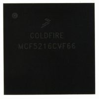
MCF5216CVF66 Freescale Semiconductor, MCF5216CVF66 Datasheet - Page 597

MCF5216CVF66
Manufacturer Part Number
MCF5216CVF66
Description
IC MPU 32BIT COLDF 256-MAPBGA
Manufacturer
Freescale Semiconductor
Series
MCF521xr
Datasheet
1.MCF5216CVM66J.pdf
(766 pages)
Specifications of MCF5216CVF66
Core Processor
Coldfire V2
Core Size
32-Bit
Speed
66MHz
Connectivity
CAN, EBI/EMI, I²C, SPI, UART/USART
Peripherals
DMA, LVD, POR, PWM, WDT
Number Of I /o
142
Program Memory Size
512KB (512K x 8)
Program Memory Type
FLASH
Ram Size
64K x 8
Voltage - Supply (vcc/vdd)
2.7 V ~ 3.6 V
Data Converters
A/D 8x12b
Oscillator Type
Internal
Operating Temperature
-40°C ~ 85°C
Package / Case
256-MAPBGA
Controller Family/series
ColdFire
Ram Memory Size
64KB
Embedded Interface Type
CAN, I2C, SPI, UART
No. Of Pwm Channels
8
Operating Temperature Range
-40°C To +85°C
No. Of Pins
256
Rohs Compliant
No
Package
256MA-BGA
Device Core
ColdFire
Family Name
MCF521x
Maximum Speed
66 MHz
Operating Supply Voltage
3.3 V
Data Bus Width
32 Bit
Number Of Programmable I/os
142
Interface Type
QSPI/UART/I2C/CAN
On-chip Adc
8-chx10-bit
Number Of Timers
8
Lead Free Status / RoHS Status
Contains lead / RoHS non-compliant
Eeprom Size
-
Available stocks
Company
Part Number
Manufacturer
Quantity
Price
Company:
Part Number:
MCF5216CVF66
Manufacturer:
FSC
Quantity:
1 670
Company:
Part Number:
MCF5216CVF66
Manufacturer:
Freescale Semiconductor
Quantity:
10 000
Part Number:
MCF5216CVF66
Manufacturer:
FREESCALE
Quantity:
20 000
Company:
Part Number:
MCF5216CVF66J
Manufacturer:
Freescale Semiconductor
Quantity:
10 000
- Current page: 597 of 766
- Download datasheet (9Mb)
A time separator is provided between the triggers and the end of conversion (EOC). The relationship to
QCLK displayed is not guaranteed.
CWPQ1 and CWPQ2 typically lag CWP and only match CWP when the associated queue is inactive.
Another way to view CWPQ1 and CWPQ2 is that these registers update when EOC triggers the write to
the result register.
For the CCW with the pause bit set (CCW0), CWP does not increment until triggered. For the CCW with
the pause bit clear (CCW1), the CWP increments with the EOC.
The conversion results Q1 RESx show the result associated with CCWx, such that R0 represents the result
associated with CCW0.
Figure 28-47
example 1 except:
When the gate closes and opens again, the conversions start with the first CCW in Q1.
When the gate closes, the active conversion completes before the queue goes idle.
When Q1 completes, both the CF1 bit sets and the SSE bit clears.
In this mode, the PF1 bit sets to reflect that a gate closing occurred before the queue completed.
Figure 28-48
assumptions as in
Freescale Semiconductor
•
•
•
CWPQ1
Q1 RES
CONVERSION TIME
TRIG1
QCLK
No pause bits set in any CCW
Externally gated single scan mode for Q1
Single scan enable bit (SSE1) is set.
CWP
EOC
QS
= 14 QCLKS
shows the timing for conversions in externally gated single-scan with same assumptions in
shows the timing for conversions in externally gated continuous scan mode with the same
LAST
0
Figure
Figure 28-46. External Positive Edge Trigger Mode Timing with Pause
LAST
MCF5282 and MCF5216 ColdFire Microcontroller User’s Manual, Rev. 3
28-47.
8
TIME BETWEEN
TRIGGERS
CCW0
4
CCW0
R0
Queued Analog-to-Digital Converter (QADC)
CCW1
CONVERSION TIME
= 14 QCLKS
8
CCW2
CCW1
R1
28-59
Related parts for MCF5216CVF66
Image
Part Number
Description
Manufacturer
Datasheet
Request
R
Part Number:
Description:
Manufacturer:
Freescale Semiconductor, Inc
Datasheet:
Part Number:
Description:
Manufacturer:
Freescale Semiconductor, Inc
Datasheet:
Part Number:
Description:
Manufacturer:
Freescale Semiconductor, Inc
Datasheet:
Part Number:
Description:
Manufacturer:
Freescale Semiconductor, Inc
Datasheet:
Part Number:
Description:
Manufacturer:
Freescale Semiconductor, Inc
Datasheet:
Part Number:
Description:
Manufacturer:
Freescale Semiconductor, Inc
Datasheet:
Part Number:
Description:
Manufacturer:
Freescale Semiconductor, Inc
Datasheet:
Part Number:
Description:
Manufacturer:
Freescale Semiconductor, Inc
Datasheet:
Part Number:
Description:
Manufacturer:
Freescale Semiconductor, Inc
Datasheet:
Part Number:
Description:
Manufacturer:
Freescale Semiconductor, Inc
Datasheet:
Part Number:
Description:
Manufacturer:
Freescale Semiconductor, Inc
Datasheet:
Part Number:
Description:
Manufacturer:
Freescale Semiconductor, Inc
Datasheet:
Part Number:
Description:
Manufacturer:
Freescale Semiconductor, Inc
Datasheet:
Part Number:
Description:
Manufacturer:
Freescale Semiconductor, Inc
Datasheet:
Part Number:
Description:
Manufacturer:
Freescale Semiconductor, Inc
Datasheet:


