MFRC53001T/0FE,112 NXP Semiconductors, MFRC53001T/0FE,112 Datasheet - Page 113
MFRC53001T/0FE,112
Manufacturer Part Number
MFRC53001T/0FE,112
Description
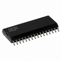
IC MIFARE HS READER 32-SOIC
Manufacturer
NXP Semiconductors
Series
MIFARE®r
Specifications of MFRC53001T/0FE,112
Rf Type
Read Only
Frequency
13.56MHz
Features
ISO14443-A, ISO14443-B, ISO15693
Package / Case
32-SOIC (0.300", 7.50mm Width)
Product
RFID Readers
Operating Temperature Range
- 25 C to + 85 C
Lead Free Status / RoHS Status
Lead free / RoHS Compliant
Lead Free Status / RoHS Status
Lead free / RoHS Compliant, Lead free / RoHS Compliant
Other names
568-2223-5
935269692112
MFRC530
MFRC53T0FED
935269692112
MFRC530
MFRC53T0FED
Available stocks
Company
Part Number
Manufacturer
Quantity
Price
Company:

Part Number:
MFRC53001T/0FE,112
Manufacturer:
MICROCHIP
Quantity:
12 000


NXP Semiconductors
24. Contents
1
2
3
3.1
4
5
6
7
8
8.1
9
9.1
9.1.1
9.1.2
9.1.3
9.1.3.1
9.1.3.2
9.1.3.3
9.1.4
9.1.4.1
9.1.4.2
9.2
9.2.1
9.2.2
9.2.2.1
9.2.2.2
9.2.2.3
9.2.3
9.2.3.1
9.2.3.2
9.3
9.3.1
9.3.1.1
9.3.2
9.3.3
9.3.4
9.4
9.4.1
9.4.2
9.4.2.1
9.4.2.2
9.4.3
9.4.4
MFRC530_33
Product data sheet
PUBLIC
Introduction . . . . . . . . . . . . . . . . . . . . . . . . . . . . 1
General description . . . . . . . . . . . . . . . . . . . . . . 1
Features and benefits . . . . . . . . . . . . . . . . . . . . 2
Applications . . . . . . . . . . . . . . . . . . . . . . . . . . . . 2
Quick reference data . . . . . . . . . . . . . . . . . . . . . 3
Ordering information . . . . . . . . . . . . . . . . . . . . . 3
Block diagram . . . . . . . . . . . . . . . . . . . . . . . . . . 4
Pinning information . . . . . . . . . . . . . . . . . . . . . . 5
Functional description . . . . . . . . . . . . . . . . . . . 7
Overview of supported microprocessor
interfaces . . . . . . . . . . . . . . . . . . . . . . . . . . . . . 7
Automatic microprocessor interface detection . 7
Connection to different microprocessor types . 8
Separate read and write strobe . . . . . . . . . . . . 8
Common read and write strobe . . . . . . . . . . . . 9
Common read and write strobe: EPP with
handshake . . . . . . . . . . . . . . . . . . . . . . . . . . . . 9
Serial Peripheral Interface . . . . . . . . . . . . . . . . 9
Memory organization of the EEPROM . . . . . . 12
Product information field (read only). . . . . . . . 13
Register initialization files (read/write) . . . . . . 13
StartUp register initialization file (read/write) . 13
Factory default StartUp register initialization
file . . . . . . . . . . . . . . . . . . . . . . . . . . . . . . . . . . 14
Register initialization file (read/write) . . . . . . . 15
Crypto1 keys (write only) . . . . . . . . . . . . . . . . 15
Storage of keys in the EEPROM . . . . . . . . . . 16
Controlling the FIFO buffer . . . . . . . . . . . . . . . 17
Interrupt request system . . . . . . . . . . . . . . . . . 18
Interrupt request handling. . . . . . . . . . . . . . . . 19
Controlling interrupts and getting their status . 19
Accessing the interrupt registers . . . . . . . . . . 19
Register overview interrupt request system . . 20
General . . . . . . . . . . . . . . . . . . . . . . . . . . . . . . . 2
Pin description . . . . . . . . . . . . . . . . . . . . . . . . . 5
Digital interface . . . . . . . . . . . . . . . . . . . . . . . . . 7
SPI read data . . . . . . . . . . . . . . . . . . . . . . . . . 10
SPI write data . . . . . . . . . . . . . . . . . . . . . . . . . 11
Key format . . . . . . . . . . . . . . . . . . . . . . . . . . . 15
FIFO buffer . . . . . . . . . . . . . . . . . . . . . . . . . . . 16
Accessing the FIFO buffer . . . . . . . . . . . . . . . 16
Access rules . . . . . . . . . . . . . . . . . . . . . . . . . . 16
FIFO buffer status information . . . . . . . . . . . . 17
FIFO buffer registers and flags . . . . . . . . . . . . 18
Interrupt sources overview . . . . . . . . . . . . . . . 18
Configuration of pin IRQ . . . . . . . . . . . . . . . . . 20
All information provided in this document is subject to legal disclaimers.
Rev. 3.3 — 6 July 2010
057433
9.5
9.5.1
9.5.1.1
9.5.1.2
9.5.1.3
9.5.1.4
9.5.2
9.5.2.1
9.5.2.2
9.5.2.3
9.5.3
9.6
9.6.1
9.6.2
9.6.3
9.6.4
9.7
9.7.1
9.7.2
9.7.3
9.7.4
9.8
9.9
9.9.1
9.9.2
9.9.3
9.9.3.1
9.9.3.2
9.9.3.3
9.9.4
9.10
9.10.1
9.10.2
9.10.2.1
9.10.2.2
9.10.2.3
9.10.2.4
9.11
9.11.1
9.11.2
9.11.2.1
9.11.2.2
9.12
9.13
9.13.1
9.13.2
Timer unit . . . . . . . . . . . . . . . . . . . . . . . . . . . . 21
Timer unit implementation . . . . . . . . . . . . . . . 21
Timer unit block diagram . . . . . . . . . . . . . . . . 21
Controlling the timer unit . . . . . . . . . . . . . . . . 22
Timer unit clock and period . . . . . . . . . . . . . . 23
Timer unit status. . . . . . . . . . . . . . . . . . . . . . . 23
Using the timer unit functions. . . . . . . . . . . . . 24
Time-out and WatchDog counters . . . . . . . . . 24
Programmable one shot timer and periodic
trigger. . . . . . . . . . . . . . . . . . . . . . . . . . . . . . . 24
Timer unit registers . . . . . . . . . . . . . . . . . . . . 24
Power reduction modes . . . . . . . . . . . . . . . . . 25
Hard power-down. . . . . . . . . . . . . . . . . . . . . . 25
Soft power-down mode . . . . . . . . . . . . . . . . . 25
Standby mode . . . . . . . . . . . . . . . . . . . . . . . . 26
Automatic receiver power-down. . . . . . . . . . . 26
StartUp phase . . . . . . . . . . . . . . . . . . . . . . . . 26
Hard power-down phase . . . . . . . . . . . . . . . . 26
Reset phase. . . . . . . . . . . . . . . . . . . . . . . . . . 26
Initialization phase . . . . . . . . . . . . . . . . . . . . . 27
Initializing the parallel interface type . . . . . . . 27
Oscillator circuit . . . . . . . . . . . . . . . . . . . . . . . 27
Transmitter pins TX1 and TX2 . . . . . . . . . . . . 28
Configuring pins TX1 and TX2. . . . . . . . . . . . 28
Antenna operating distance versus power
consumption. . . . . . . . . . . . . . . . . . . . . . . . . . 28
Antenna driver output source resistance . . . . 29
Source resistance table . . . . . . . . . . . . . . . . . 29
Calculating the relative source resistance . . . 30
Calculating the effective source resistance . . 30
Pulse width. . . . . . . . . . . . . . . . . . . . . . . . . . . 30
Receiver circuit . . . . . . . . . . . . . . . . . . . . . . . 31
Receiver operation. . . . . . . . . . . . . . . . . . . . . 31
Automatic Q-clock calibration . . . . . . . . . . . . 32
Amplifier . . . . . . . . . . . . . . . . . . . . . . . . . . . . . 33
Correlation circuitry . . . . . . . . . . . . . . . . . . . . 33
Serial signal switch . . . . . . . . . . . . . . . . . . . . 34
Serial signal switch block diagram . . . . . . . . . 34
Serial signal switch registers . . . . . . . . . . . . . 35
Active antenna concept . . . . . . . . . . . . . . . . . 36
Driving both RF parts . . . . . . . . . . . . . . . . . . . 37
MIFARE higher baud rates. . . . . . . . . . . . . . . 37
MIFARE authentication and Crypto1 . . . . . . . 37
Crypto1 key handling . . . . . . . . . . . . . . . . . . . 38
Stopwatch . . . . . . . . . . . . . . . . . . . . . . . . . . . 24
Receiver circuit block diagram . . . . . . . . . . . . 31
Evaluation and digitizer circuitry . . . . . . . . . . 33
Authentication procedure . . . . . . . . . . . . . . . . 38
ISO/IEC 14443 A Reader IC
MFRC530
© NXP B.V. 2010. All rights reserved.
continued >>
113 of 115
Related parts for MFRC53001T/0FE,112
Image
Part Number
Description
Manufacturer
Datasheet
Request
R

Part Number:
Description:
IC READER 13.56MHZ 32-SOIC
Manufacturer:
NXP Semiconductors
Datasheet:

Part Number:
Description:
Iso/iec 14443 A Reader Ic
Manufacturer:
NXP Semiconductors
Datasheet:
Part Number:
Description:
NXP Semiconductors designed the LPC2420/2460 microcontroller around a 16-bit/32-bitARM7TDMI-S CPU core with real-time debug interfaces that include both JTAG andembedded trace
Manufacturer:
NXP Semiconductors
Datasheet:

Part Number:
Description:
NXP Semiconductors designed the LPC2458 microcontroller around a 16-bit/32-bitARM7TDMI-S CPU core with real-time debug interfaces that include both JTAG andembedded trace
Manufacturer:
NXP Semiconductors
Datasheet:
Part Number:
Description:
NXP Semiconductors designed the LPC2468 microcontroller around a 16-bit/32-bitARM7TDMI-S CPU core with real-time debug interfaces that include both JTAG andembedded trace
Manufacturer:
NXP Semiconductors
Datasheet:
Part Number:
Description:
NXP Semiconductors designed the LPC2470 microcontroller, powered by theARM7TDMI-S core, to be a highly integrated microcontroller for a wide range ofapplications that require advanced communications and high quality graphic displays
Manufacturer:
NXP Semiconductors
Datasheet:
Part Number:
Description:
NXP Semiconductors designed the LPC2478 microcontroller, powered by theARM7TDMI-S core, to be a highly integrated microcontroller for a wide range ofapplications that require advanced communications and high quality graphic displays
Manufacturer:
NXP Semiconductors
Datasheet:
Part Number:
Description:
The Philips Semiconductors XA (eXtended Architecture) family of 16-bit single-chip microcontrollers is powerful enough to easily handle the requirements of high performance embedded applications, yet inexpensive enough to compete in the market for hi
Manufacturer:
NXP Semiconductors
Datasheet:
Part Number:
Description:
The XA-S3 device is a member of Philips Semiconductors? XA(eXtended Architecture) family of high performance 16-bitsingle-chip microcontrollers
Manufacturer:
NXP Semiconductors
Datasheet:

Part Number:
Description:
The NXP BlueStreak LH75401/LH75411 family consists of two low-cost 16/32-bit System-on-Chip (SoC) devices
Manufacturer:
NXP Semiconductors
Datasheet:
Part Number:
Description:
The NXP LPC3130/3131 combine an 180 MHz ARM926EJ-S CPU core, high-speed USB2
Manufacturer:
NXP Semiconductors
Datasheet:
Part Number:
Description:
The NXP LPC3141 combine a 270 MHz ARM926EJ-S CPU core, High-speed USB 2
Manufacturer:
NXP Semiconductors
Part Number:
Description:
The NXP LPC3143 combine a 270 MHz ARM926EJ-S CPU core, High-speed USB 2
Manufacturer:
NXP Semiconductors

Part Number:
Description:
The NXP LPC3152 combines an 180 MHz ARM926EJ-S CPU core, High-speed USB 2
Manufacturer:
NXP Semiconductors